Pages created and updated by
Terry Sturtevant
Date Posted:
September 13, 2018
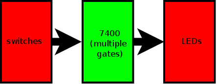
In this lab you will wire switches to NAND gates with LEDs for output.
Light Emitting Diodes,
or LED's for short, emit light when an
electric current is passed
through them. The amount of current must be limited, however, or
the diode will be destroyed.
Usually a current of 10 mA is sufficient to light a diode, so if
a 5 volt supply is being used,
a 500 resistor placed in series with the diode will provide the
right current. Note that
the diode has one long pin, called the anode, and one short pin,
called the cathode.
The longer pin is connected to the higher (i.e., more positive)
voltage, and the short
pin goes to ground.
Note in the following image, the two LEDs on the right light
with a high signal (on the yellow wires),
while the
two LEDs at the left light
with a low signal (on the orange wires).
Note that the order of the resistor and LED don't matter
as long as the circuit is connected correctly.
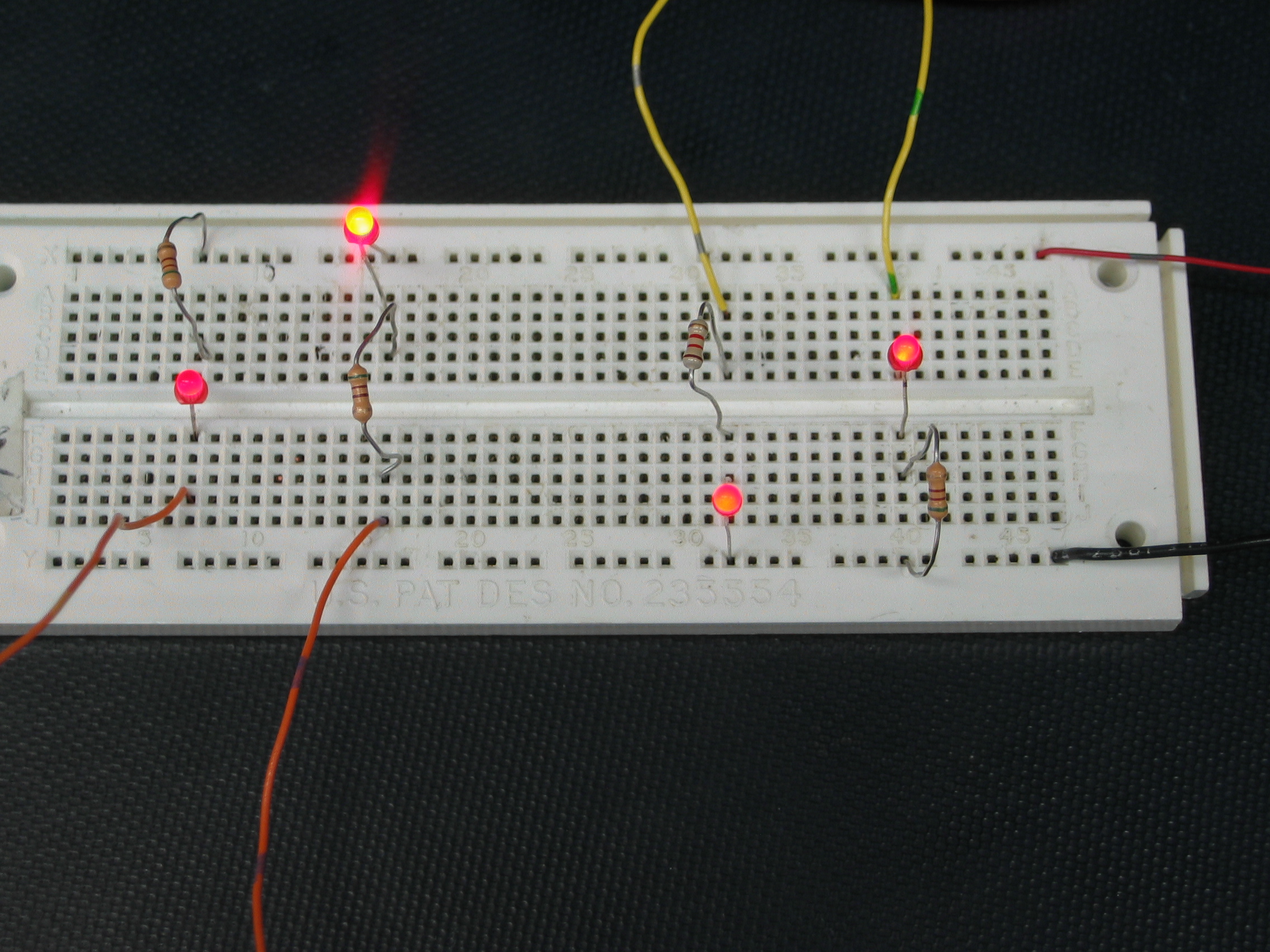
Note: You don't have to wire up all of these
different configurations; use whichever one suits the application
at hand.
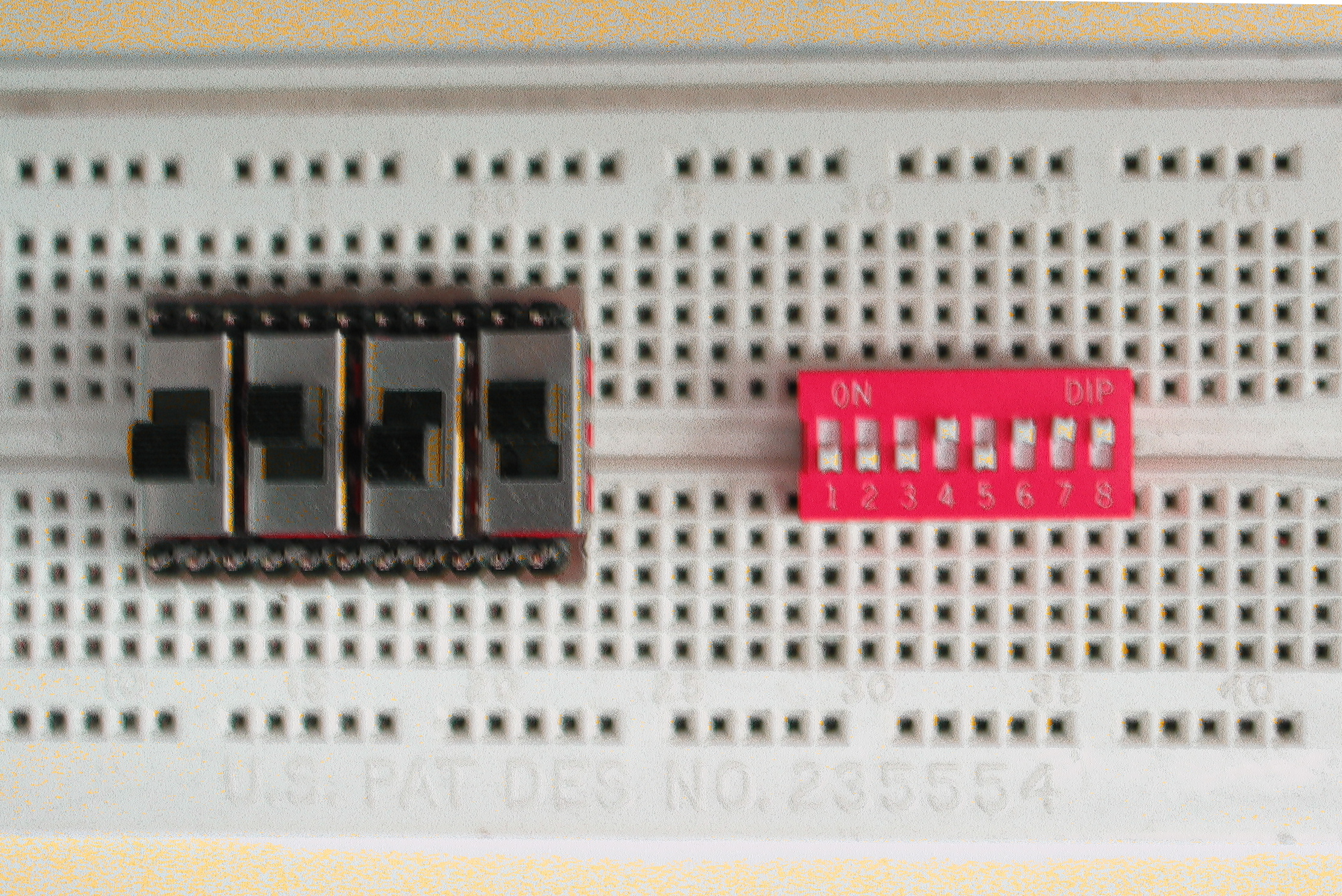
A Dual Inline
Package, or DIP
switch can be used to select between 0 and 5 volts
at some point in a circuit. Since the DIP switch does not have
any power or ground connectors
this must be done externally.
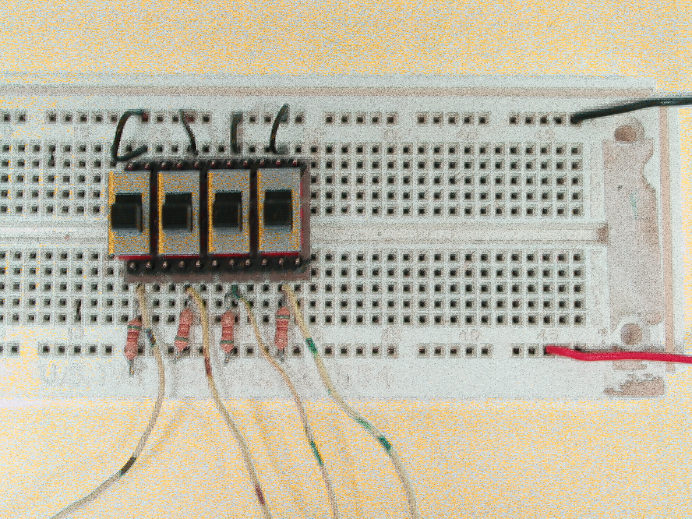
In this lab exercise, we'll use some prototype switches
instead of DIP switches because they are easier to manipulate
by hand,
even though they work exactly the same as DIP switches.
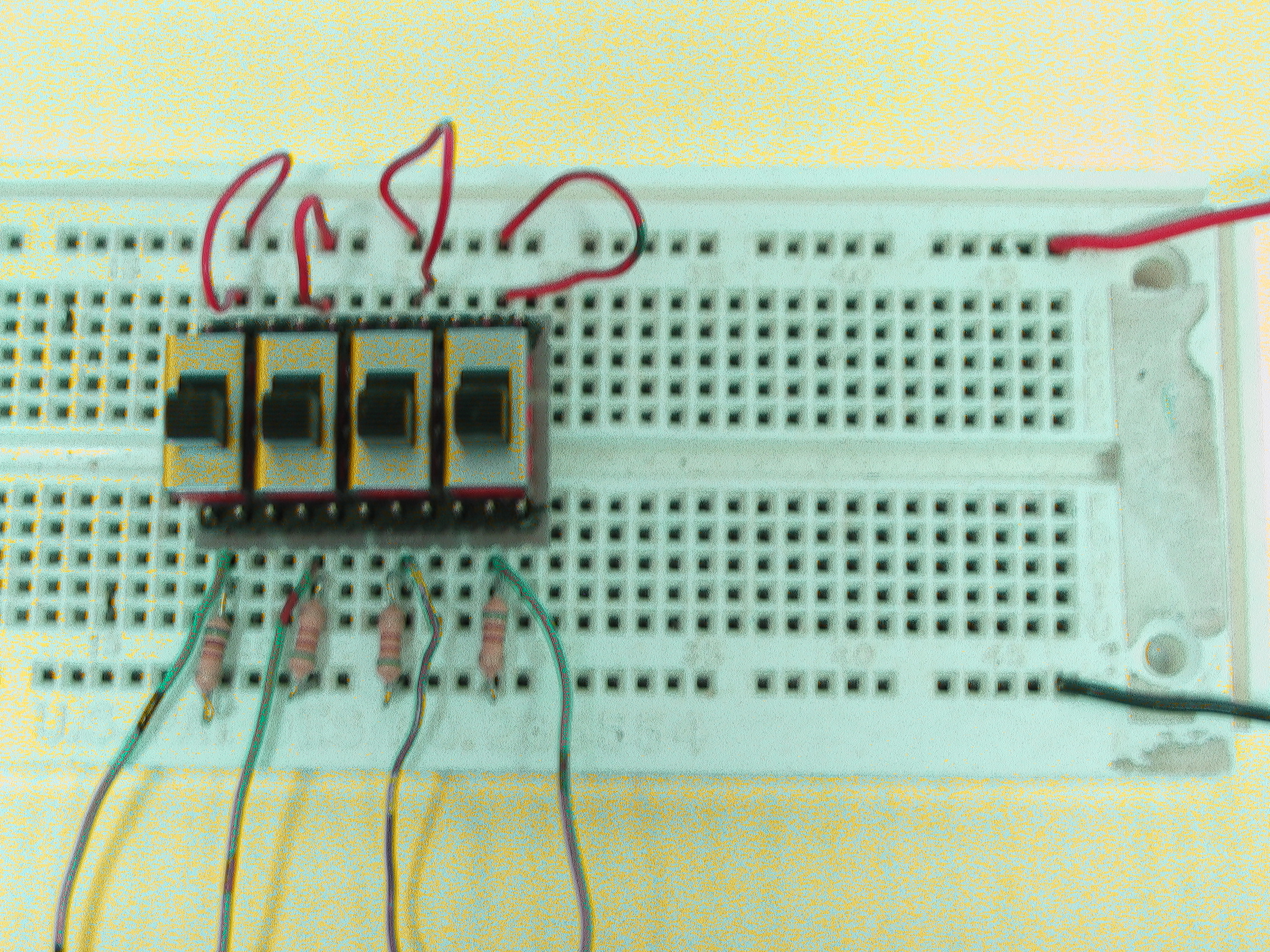
In our case we want a high (5V) when then switch is turned on,
so each input pin we are
using must be connected to power. When the switch is off we
want a low (0V); but remember
when the switch is off it is in a floating state. To resolve our
floating pins issue we need to
add a resistor from each of the output pins to ground. The
output signal comes from where the resistor and switch meet.
(In the picture below, the signal wires are green.)
In the image below, the cases have been reversed, so that when
the switch is closed,
the output is low, and when the switch is open, the output is high.
Note the
changes that happen in this case.
The yellow wires are the signals coming from the switches.
Usually it doesn't matter which switch position
(i.e. "on" or "off") gives a high,
so either setup is fine.
The output is always taken from the side of the switch with the resistor.
Since all of the points in a row are connected, the output can come from any place in the correct row.
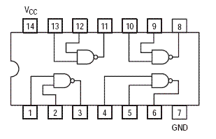
For this lab we will be using the 7400 Quad NAND gate IC. This chip contains four 2-input NAND gates. The pin numbers associated with each input and output of this chip are listed above the input and output of the NAND gates in the diagram. You can also find more information in the datasheet. The pinout is shown below.
When building a circuit with several components, it's easier to debug if you build it in a modular fashion. This circuit will be in three modules:
Here's how a modular circuit might look on a single board.
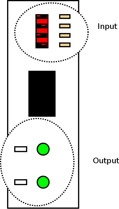
You'll build them one at a time, and as each module is known to work, use it to help test the others.
In this lab you will create a circuit which will turn an LED (light emitting diode) on or off depending on the selected input. The LEDs will give a visual indication of a 1 (LED lighted) or a 0 (LED dark). We connect the switch to select between 1 (high voltage +5v) and 0 (low voltage).
Below there is a schematic diagram for one gate of the completed circuit, but don't look at it yet. The following description of modular construction and testing applies to any circuit so that you don't waste a lot of time trying to debug a complete circuit without knowing which, if any, parts of the circuit are correct.
For debugging purposes, it's easiest to make sure your outputs work
first.
If you don't know your outputs are working, you have no way of
knowing whether the rest of your circuit is working or not.
For the output module, choose a colour of wire
other than red or black.
Once you have the output working, you can use it to test the inputs.
For the input module, choose a colour of wire
different from what you used for the output module and
black.
other than red or black.
Since you have now verified that the inputs and outputs work, you should be able to connect them to the gates to see if the gates work.
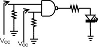
Here's the schematic for the completed circuit for one gate. The lines with arrows represent the switches. (When the switch is closed, the input will be HIGH. When the switch is open, the input will be LOW. This is called active high configuration.)
Demonstrate your results to the lab demonstrator.


![]()
Wilfrid Laurier University
© 2019 Wilfrid Laurier University