Pages created and updated by Terry Sturtevant Date Posted: September 18, 2017


PC/CP220 Digital Electronics Lab

Introducing Integrated Circuits

Objective:

Background:

In this PC/CP220 lab we'll walk you through wiring a simple gate circuit using one specific integrated circuit (IC), the 7400 chip.


basic circuit

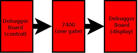
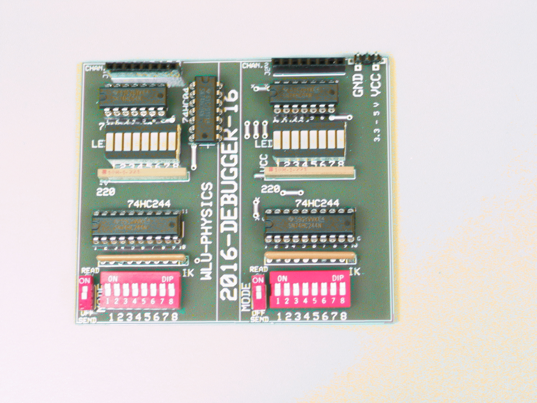
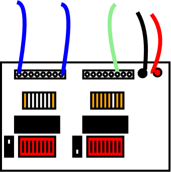
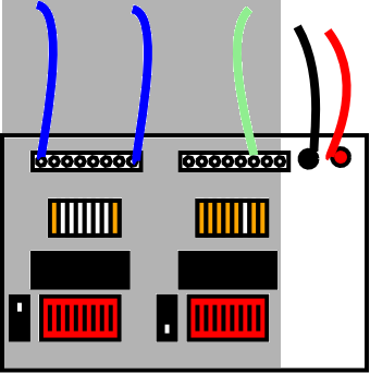
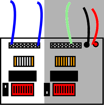
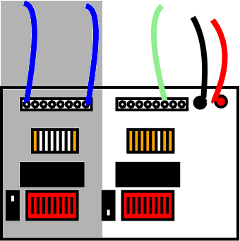
You'll use a debugger board for input and output.

It's a good introduction to some of the more complex logic chips that you'll be using later in the lab.

The 7400 device is part of the 74xx family of integrated circuits. (The xx refers to the fact that there are many possible numbers which follow the 74.) For more info about the 74xx family see the 7400 series entry in Wikipedia.

IC pin numbering and orientation

NAND chip

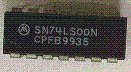
Locate the 7400 chip/IC in your lab kit. This chip has something like SN74LS00N written on it. Note that there are 5 parts to the chip "number":

  1. A text prefix; eg. SN
    • This indicates the manufacturer
  2. The numbers 74
    • This indicates the logic family;
    • in this case, normal TTL
    • (54 would indicate military-spec TTL)
  3. More text; eg. LS
    • This indicates the sub-family
    • (You may even see chips with no letters here, meaning the original "plain" TTL.)
  4. More numbers; e.g. 00
    • This indicates the specific device;
    • in this case, a quad 2 input NAND gate
  5. A text suffix; eg. N
    • This indicates the package type
    • (This will indicate which version of the pinout applies to this chip.)

Normally you will just refer to the device by using the two sets of numbers, such as 7400, and ignore the letters.

The LS tells you that it is a low power Schottky chip. The manufacturer includes other information along with the 74LS00 on the chip.


Reading a pinout diagram

This is a Dual-Inline Package (DIP), referring to the chip's two rows of pins. Notice that this chip has fourteen pins. If you want to use an IC chip, then you will always need to know the pinout. That's the electrical engineering term for describing the way the pins are connected to the internal circuitry of the chip. You need to know where the power supply is connected and where the gate inputs and outputs are connected.

How do you know the IC pinout? You will need to look at the IC's datasheet. The manufacturer provides you with the IC datasheets for all of their products. See 7400 datasheet for an example.

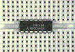
Here's a picture of the 7400 chip in a circuit board:

NAND on board

and here's the pinout for a 7400 chip:

NAND pin description

Identifying pin 1

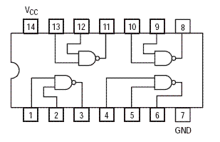
How do you know which pin is "pin 1" on the IC? You will find either a circle marking the first pin or a semicircle marking the top of chip. The pins on an N-pin DIP are numbered as shown :
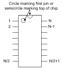
Dual-Inline Package Chip.

Testing a NAND gate

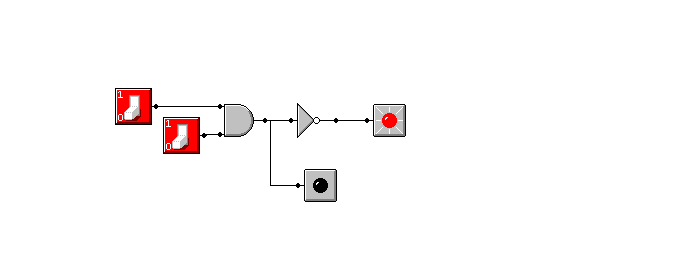
The output of a NAND gate should be HIGH unless both inputs are HIGH. (This is the opposite of an AND gate where the output should be LOW unless both inputs are high.) The animation below illustrates both of these.

NAND operation

Task:

Parts List

Becoming Familiar with Integrated Circuits

  1. Verify that you have the right chip.
  2. Identify pin 1.
  3. Connect power and ground to the breadboard and the debugger board.
  4. Identify the power and ground pins on the chip and connect power and ground from the breadboard.
  5. Choose one of the 4 gates on the chip, and wire the inputs and output to the debugger board. Note that you will have to use pins from two separate banks on the debugger board. One bank will be in "control" mode to provide input to your chip, and the other bank will be in "display" mode to observe the output of your chip.
  6. Test the four possible input combinations to the gate to show that the output is as expected.

Using the debugger board

The debugger board looks like this:
debugger picture
Here's what the debugger board looks like connected:
debugger board

These are the power connections:
debugger board 
power 
    connections

This is a bank in "control" mode (i.e. you can use it for inputs to a circuit):
debugger board 
    control mode bank
Hint: If you're not using all of the pins in one bank, spread them out so it's easier to tell which is which.

This is a bank in "display" mode (i.e. you can use it to see the outputs from a circuit):
debugger board 
     display mode bank

Demonstrate and explain your results to the lab demonstrator.

Resources

To view pdf documents, you can download Adobe Acrobat Reader .
get Acrobat Reader
If you need to update a browser, you might try Firefox which is Get Firefox!
Since this page uses cascading style sheets for its layout, it will look best with a browser which supports the specifications as fully as possible.

If you are looking for an office package, with a word processor, spreadsheet, etc., you might try LibreOffice which is Get LibreOffice!

Go to the main page for the Department of Physics and Computer Science.

Valid XHTML 1.1

Valid CSS!

WCAG 2.0
(Level AA)

Wilfrid Laurier University