PC/CP200 Electronics Lab I
Logic Gates Characteristics - Tri-state
Outputs
Objectives
- To gain more experience with an oscilloscope.
- To investigate the operation of tri-state gates.
Preparation
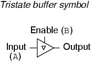
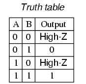
Tri-state gates can output one of three values: logic
high, logic low, or high impedance (Z or High-Z). The high
impedance state behaves like an 'open'.
Equipment
- bench power
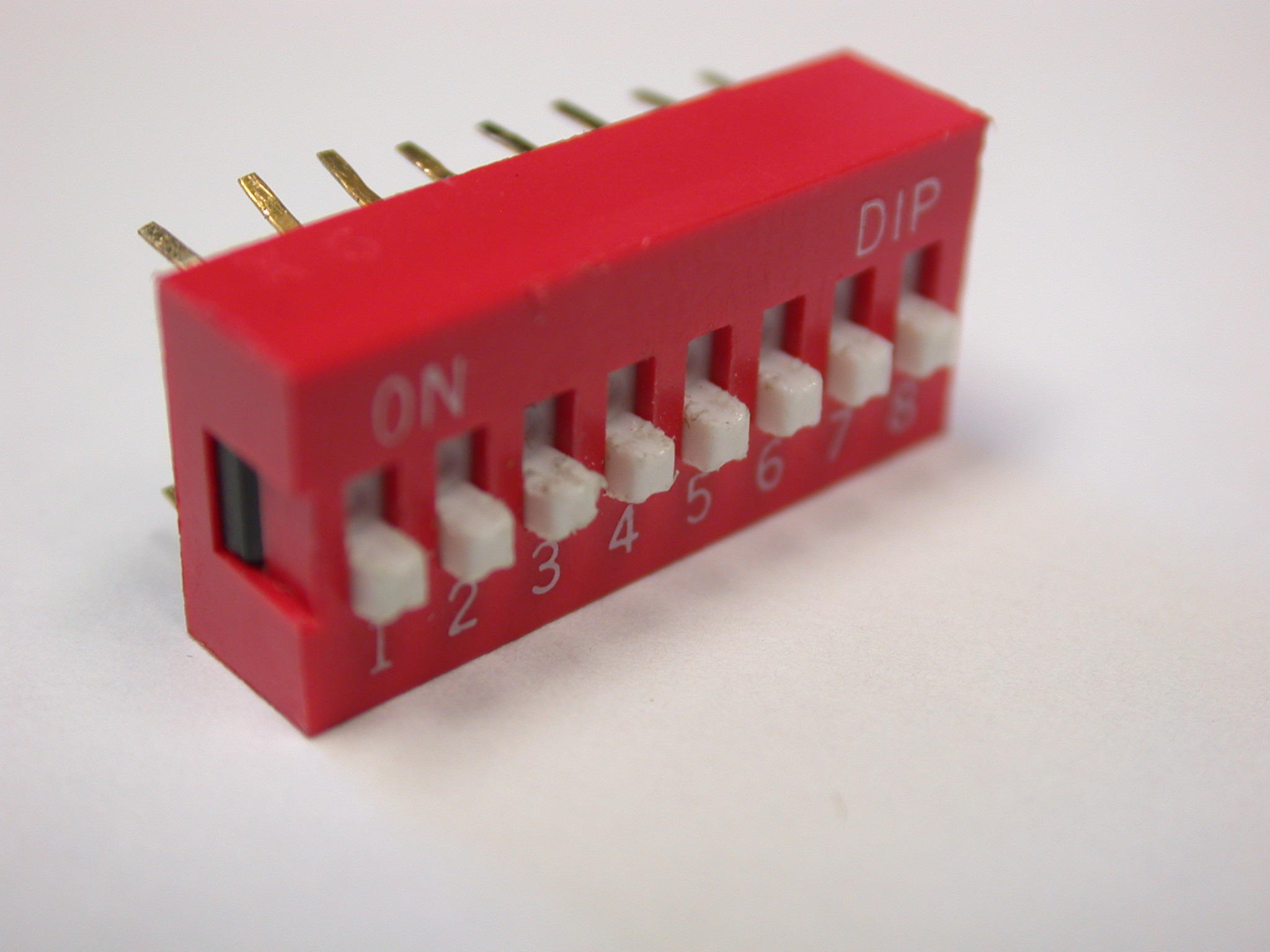
- breadboard, resistors, resistor arrays, bargraph LED,
DIP switch bank
- 74LS244
- signal/function generator
- oscilloscope
Procedure
- Connect a function generator to the oscilloscope, and set it
up to produce a 0 to 5V square wave output.
Make sure the output from the function
generator is from 0 to 5 V; the normal DC offset may have the
signal centred around 0V, and the normal amplitude may not be
correct.
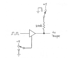
- Construct the circuit shown below using one buffer on the
DM74LS244 Octal 3-STATE Buffer. Test your circuit by driving the
input with the function generator.
Watch the effect of the
ENABLE. When the tri-state is disabled, the 100k resistor should
determine the output level. When the tri-state is enabled, the
tri-state should drive the square wave onto the output line. Note
that the 100k pull-up/down resistor is included to demonstrate
the high impedance state; without it, there is no way to see
'floating'.
Demonstrate the operation of your circuit to the lab
staff.
- To demonstrate the usefulness of the tri-state output, you
will construct a mini debugger board that functions exactly like
the prefabricated ones that you have used in our labs. Feel free
to look at our debugger boards.
You may need to remind yourself about how to wire up DIP
switches
and
bargraph
LEDs
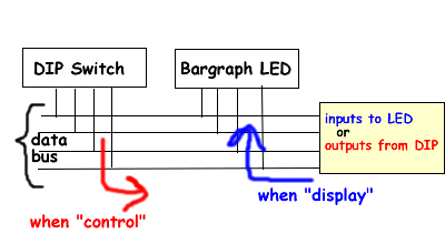
Your mini debugger board will consist of 4 bits that can be
configured to either "display" logic levels in a
circuit or to "control" logic levels to a circuit. In
"display" mode, a signal at an input pin will turn
the corresponding LED ON if the signal is HIGH and OFF if it is
LOW. In "control" mode, the DIP switches for a bank
of connectors will control the logic level on the data bus.
Switching from one mode to the other is accomplished either by a
single DIP switch or by a jumper. A block diagram of the system
is shown below. The block diagram does not include the resistor
arrays required by the bargraph LED and DIP
switch. Nor does the block diagram show the location of the
tri-state buffers.
Should the buffer go here?
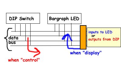
Or here?
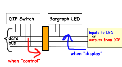
Or here?
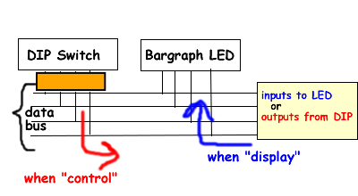
Or here?
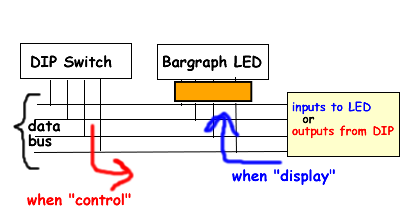
For this application, the tri-state buffer will be used to
electrically 'disengage' competing users of the shared
bus. Where do the buffers have to be located? Hint: who is
putting data on the data bus? What is the relationship of the
buffers to the 'control' and 'display'
signals? To improve reliability, it would be desirable to ensure
that 'control' and 'display' cannot both be
in effect at the same time.
To make testing easier, get the output (i.e. LED + resistor
array) portion working first, then get the input (i.e. dip switch
+
resistor array) portion working, since you'll be able to use the
output portion to help testing the input!
Demonstrate the operation of your circuit to the lab
staff.
Wilfrid Laurier University
© 2019 Wilfrid Laurier University


