Cyclic Redundancy Check (CRC)
PRELAB
This week's laboratory investigates cyclic redundancy checking (CRC). CRC code generation is an important tool in computer networking at the data link layer level, since it is at that level that error detection is done by hardware. At a higher layer (transport), error detection is done in software, using a much simpler algorithm to allow speedy processing. In all cases, error detection provides an efficient means of implementing error control for reliable transmission of messages.
Polynomial Arithmetic for CRC Generation
The CRC, or frame check sequence R, is the remainder
of the following binary division:
![]() . M is a k-bit message,
and P is a generating polynomial of degree n.
The remainder, R, is then appended to the message
M to form a (k + n)-bit
frame T to be transmitted.
. M is a k-bit message,
and P is a generating polynomial of degree n.
The remainder, R, is then appended to the message
M to form a (k + n)-bit
frame T to be transmitted.
Polynomial Arithmetic for CRC Reception
At the receiver, the received frame T is divided by the same generating polynomial P. A remainder of 0 indicates no error. Any other remainder is an indication of a burst error. Codes that are generated using shiftback registers and based on generating polynomials can detect 100% of all burst errors up to length n, that is, up to n bits in error, where n is the degree of the generating polynomial P. Higher burst lengths can also be detected, but at a lesser percentage.
- Use modulo-2 polynomial arithmetic to compute the CRC code which will be
sent along with the following 12-bit message: M=110011101011. The generating
polynomial is P(x) = x4 + x + 1.
- Determine M(x). (Eg. M = 11011, M(x) = x4 + x3 +x + 1)
- P(x) is a 4th degree polynomial, hence n = 4
- 2n x M/P = x4M(x)/P(x), since n = 4. Perform the long division. The remainder R is your CRC code. Your code must have 4 bits, since n = 4.
- Sketch your circuit based on P(x) given above in your lab book.
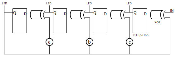
- The circuit is constructed using D flip-flops and exculsive-OR gates.
- The number of flip-flops is four, since n = 4, the degree of the generating polynomial.
- You will need an input for CLR.
- The following is a general circuit for a 4 flip-flop register based on
P(x) = x4 + ax3 + bx2 + cx + 1, where
a, b and c are 1 for feedback
(connected to final Q) and 0 for no feedback (connected to gnd).
- We will be using a debounced switch as a manual clock input. You will need the 7474 chip (D flip-flop). The input will be a wire that you manually move from ground to power to give each rising edge (clock pulse). The output will be the clock pulse into your altera board to trigger the D flip-flops in the circuit above.
- REVIEW QUARTUS II
Datasheet: 74LS74
[Copyright 1995 National Semiconductor Corporation.
Datasheet June 1989]
Datasheet: 74LS86
[Copyright 1995 National Semiconductor Corporation.
Datasheet June 1989]
Datasheet: 74LS00
[Copyright 1995 National Semiconductor Corporation.
Datasheet June 1989]
| Resistors (Ω) | Capacitors (μF) | ||
|---|---|---|---|
| 10 | 1k | 0.001 | 0.01 |
| 3.9k | 4.7k | 0.033 | 0.047 |
| 5.1k | 10k | 0.1 | 0.22 |
| 20k | 51k | 0.33 | 0.47 |
| 100k | 1M | 1 | 10 |