Programmable logic device, or PLD, is a general name for a digital integrated circuit capable of being programmed to provide a variety of different functions.
It's good for prototyping designs. Only a single chip is required to implement logic designs. It allows us to simplify designs and reduce development times. Changes in the design can be easily implemented by reprogramming the device. Simple PLDs (such as the one we use in our lab) can realize from 2 to 10 functions of 4 to 16 variables on a single integrated circuit
Step 1: Open your project. File --> Open Project
Step 2: Selecting your Device
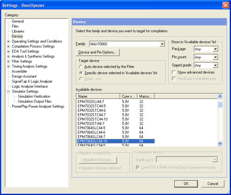
Select Assignments --> Device from the pull-down
menu. Select MAX7000S from the "Family" pull-down list.
Select the "Specific device selected" and then choose EPM7064SLC44-10, which is
the device we are using in our lab. Select "OK."

Step 3: Assigning Pins
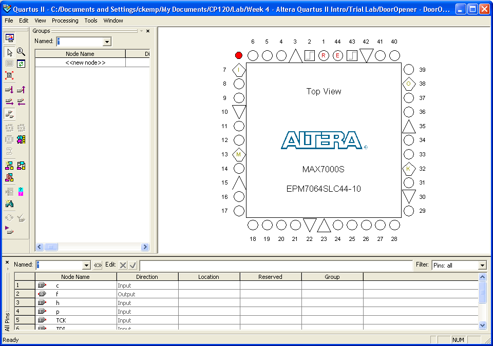
Select Assignments --> Pins from the pull-down menu.
You will notice that the pins around the edges of the chip have different symbols. The plain round circles with nothing written insied of them are used for input and output.
Select each input and output from the bottom of the screen and drag it on top of the pin you would like to use - make sure you click on the name. (ie. if you want h to be pin 4, click h on the bottom of the screen and drag it on top of the circle under the label 4). Remember, use ONLY the plain round circles!!
When you are finished you can close the window.
Step 4: Compile
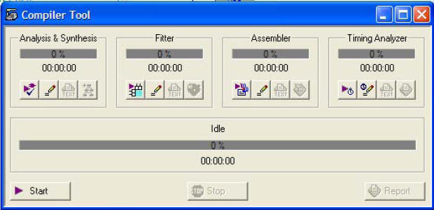
You will need to compile your design again to fit your design on the PLD board.
Click on Processing → Compiler Tool to start compilation. Then click start.
Step 5: Download your circuit to CPLD board
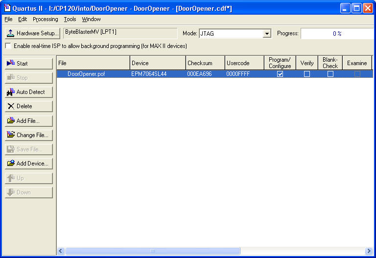
Connect CPLD board to ByteBlaster cable (connected to LPT1 on your PC).
Connect the ground and power (5v) to the CPLD board and turn the power on.
Solving the problems:
| Problem | Solution |
|---|---|
| Unable to scan device chain. | This is generally a problem with power. Check:
|
| JTAG error | This is generally a problem with the connection. Try:
|
| License error | This is generally a problem if you haven't done anything with the software recently. The server times out and loses the connection to the licencing file.
|
Step 6: Find the Pin Assignment
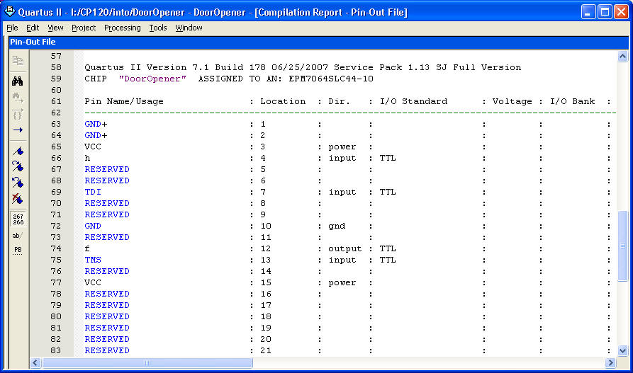
To implement the logic in a CPLD we need to know which pins in the CPLD were assigned to the input and output of the logic.
Quartus assigns the device’s pins to inputs and outputs in your design automatically if you do not assign them.
To look them up, in the main window select Processing → Compilation Report → Fitter → Pin-Out File. This is a detailed report showing where all of the pins on the CPLD have been assigned.
Step 7: Wire input and output
You can unplug the Byte Blaster cable and turn off the power while you are wiring your circuit. You will not lose your program.
Use the debugger board to wire the input (use the control mode) and the output (use the display mode). You do not have to wire the Vcc and the GND, only your inputs and outputs. (ie. c, h, p & f)
Step 8: Troubleshooting
If you smell smoke turn off the power immediately and DO NOT touch the Altera chip. It gets extremely hot if it is short circuited. Check all your power and grounds, have someone else check your power and grounds - something IS wrong!! Hopefully, your chip will still work. :)