Pages created and updated by
Terry Sturtevant
Date Posted:
October 31, 2019
To create, download and test a circuit using a CPLD and appropriate input and output devices.
In this task you'll do something like in the previous lab, but with a different circuit.
Always start by creating a new
folder.
Do not put new files in the same folder as your previous
projects!
Then create a new
project, and then create a BDF file. Do not
start by creating a BDF file.
Step 1: Look up the equation for the prime number identifier in the
sample Phase II document.
Step 2: Draw your
circuit diagram using Altera Quartus II using the
appropriate gates.
Use the recommended drawing tips.
Step 3: Download
your circuit design to the CPLD.
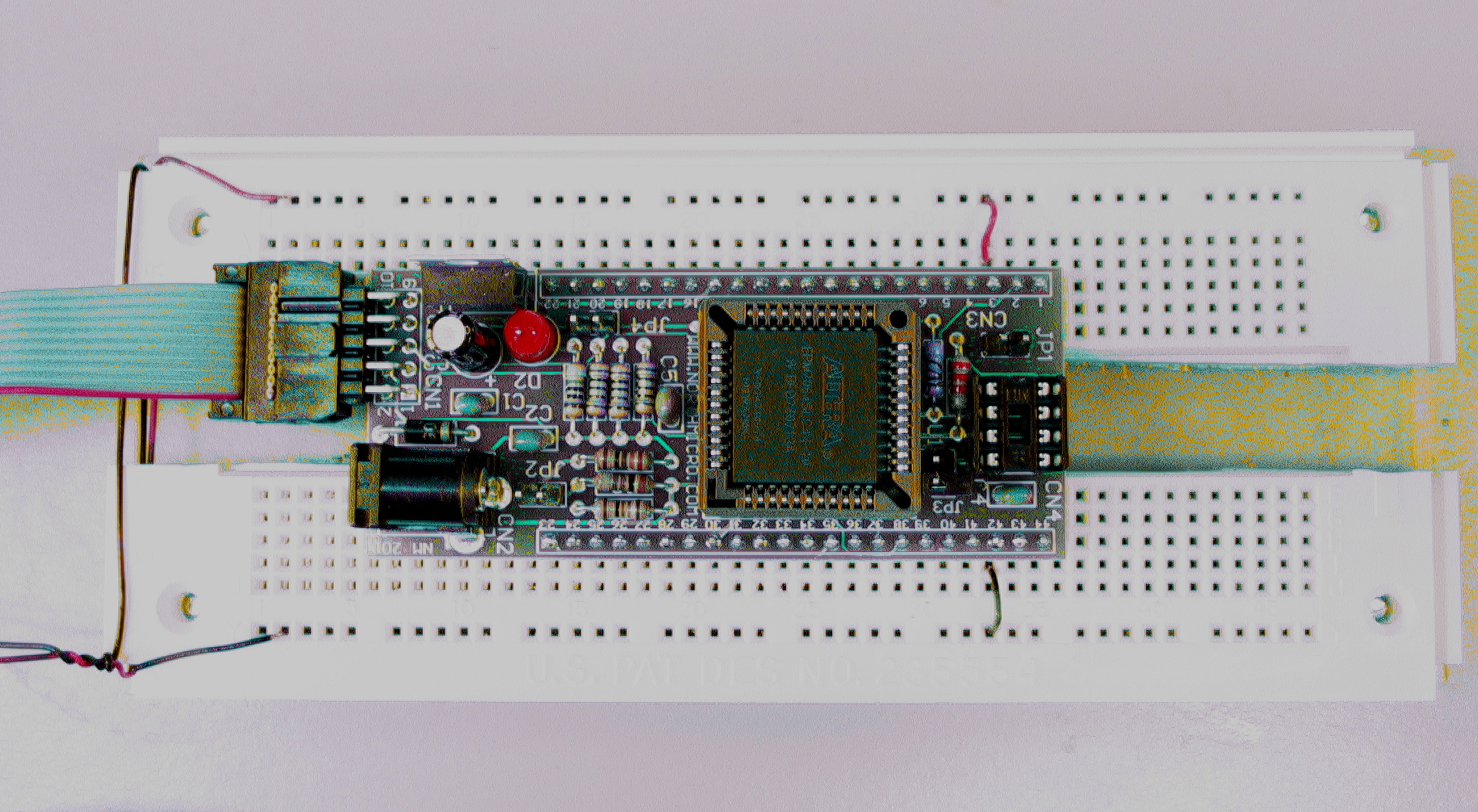
You may have a different type of CPLD board than last week.
Make sure the JTAG cable is attached correctly for whichever board
you have.
One looks like this:
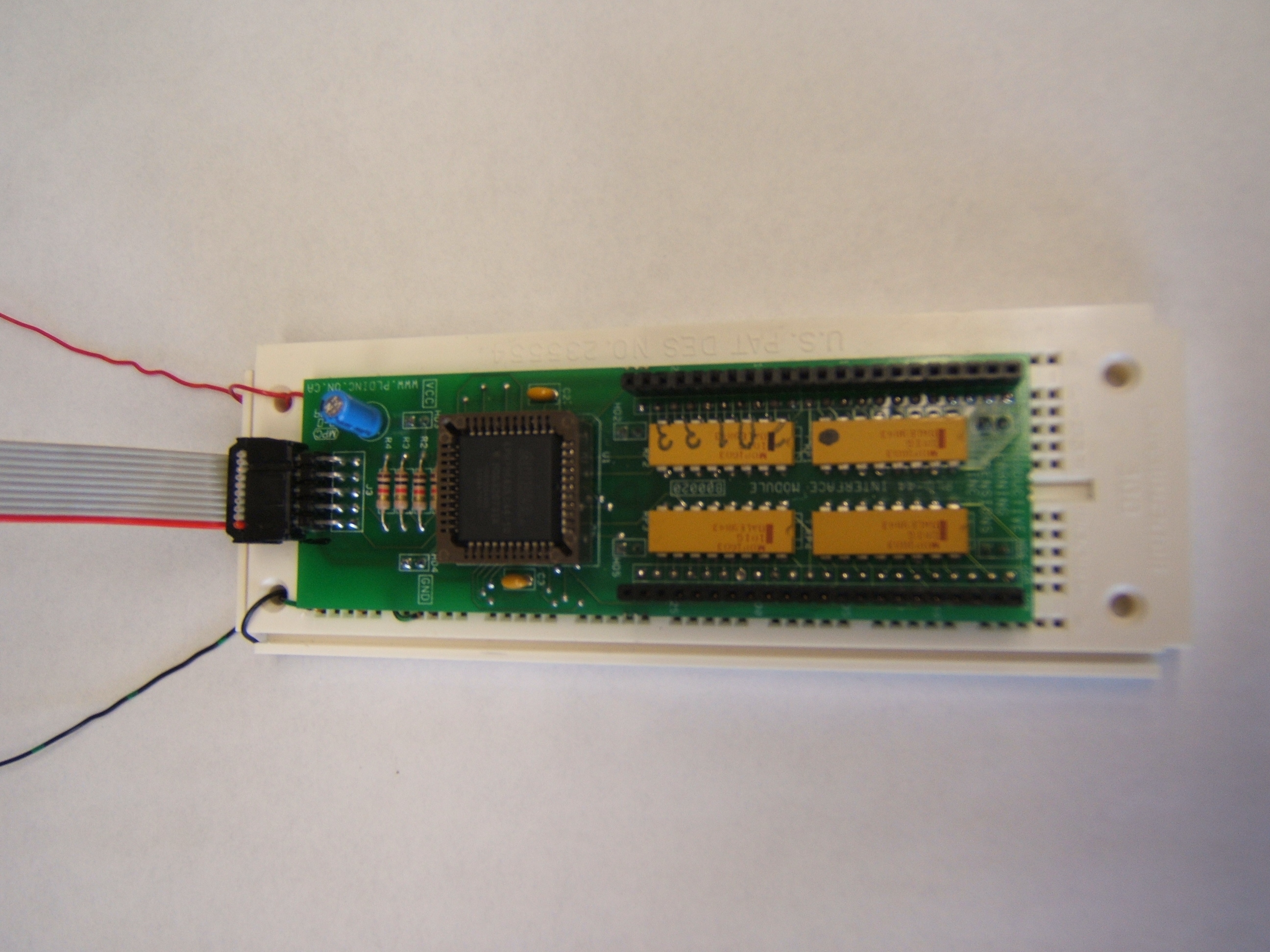
[click image to get a larger image]
The other style of CPLD board looks like this:
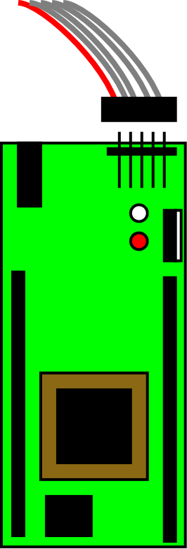
[click image to get a larger image]
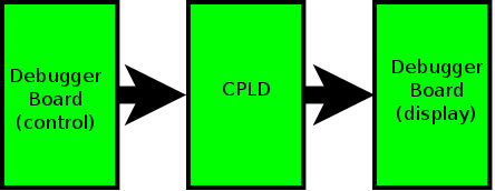
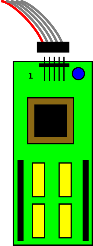
Step 4: Wire the
input and output pins using the debugger board.
Demonstrate your working prototype to the lab demonstrator.


![]()
Wilfrid Laurier University
© 2019 Wilfrid Laurier University