Pages created and updated by
Terry Sturtevant
Date Posted:
May 12, 2017
To create, download and test a circuit using a CPLD and appropriate input and output devices.
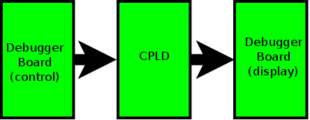
In this task you'll do something like in the previous lab, but with a different circuit.

Step 1: Look up the equation for the prime number identifier in the
sample Phase II document.
Step 2: Draw your
circuit diagram using Altera Quartus II using the
appropriate gates.
Use the recommended drawing tips.
Step 3: Download
your circuit design to the CPLD.
Assign all of your pins to fit in one "bank" of CPLD
connections, so only one jumper cable is required.
You may want to try a different bank than before.
Step 4: Wire the
input and output pins using the debugger board.
Demonstrate your working prototype to the lab demonstrator.


Wilfrid Laurier University
© 2019 Wilfrid Laurier University