Pages created and updated by
Terry Sturtevant
Date Posted:
May 12, 2017
Programmable Logic Device, or PLD, is a general name for a digital integrated circuit capable of being programmed to provide a variety of different functions.(The "C" in CPLD stands for "complex".)
A PLD is good for prototyping designs. Only a single chip is required to implement a complete logic design. It allows us to simplify designs and reduce development times. Changes in the design can be easily implemented by reprogramming the device. Simple PLDs (such as the one we use in our lab) can realize from 2 to 10 functions of 4 to 16 variables on a single integrated circuit
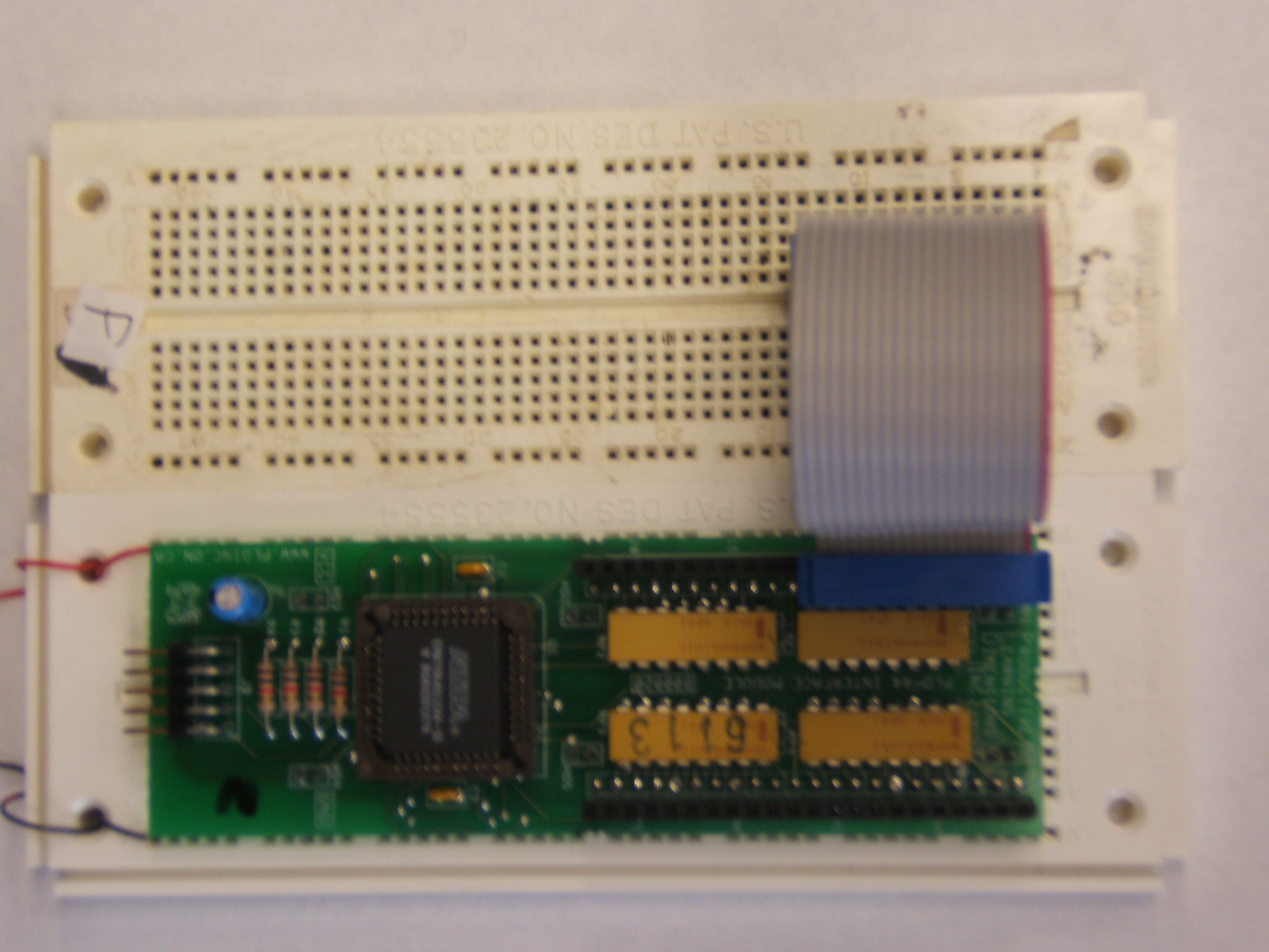
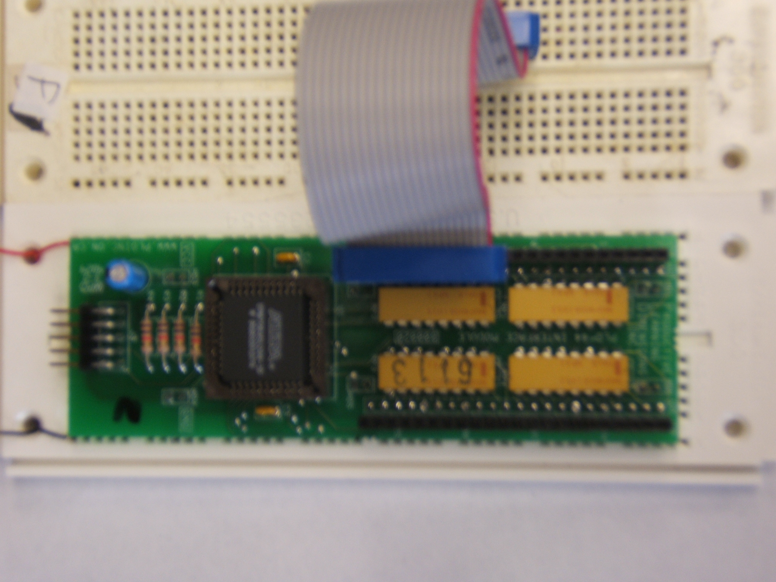
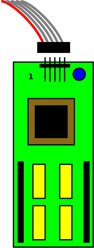
One style of CPLD board looks like this:
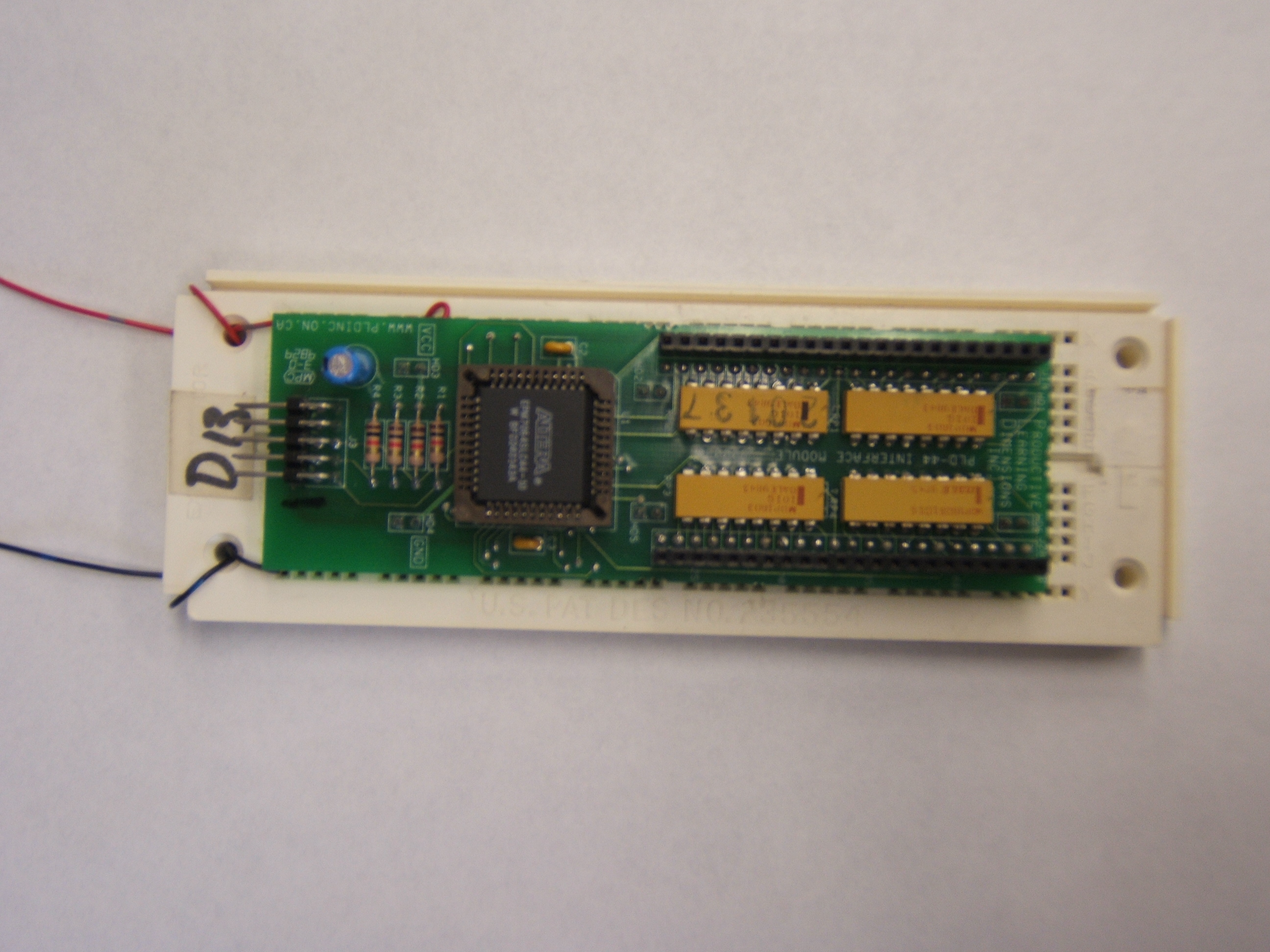
[click image to get a larger image]
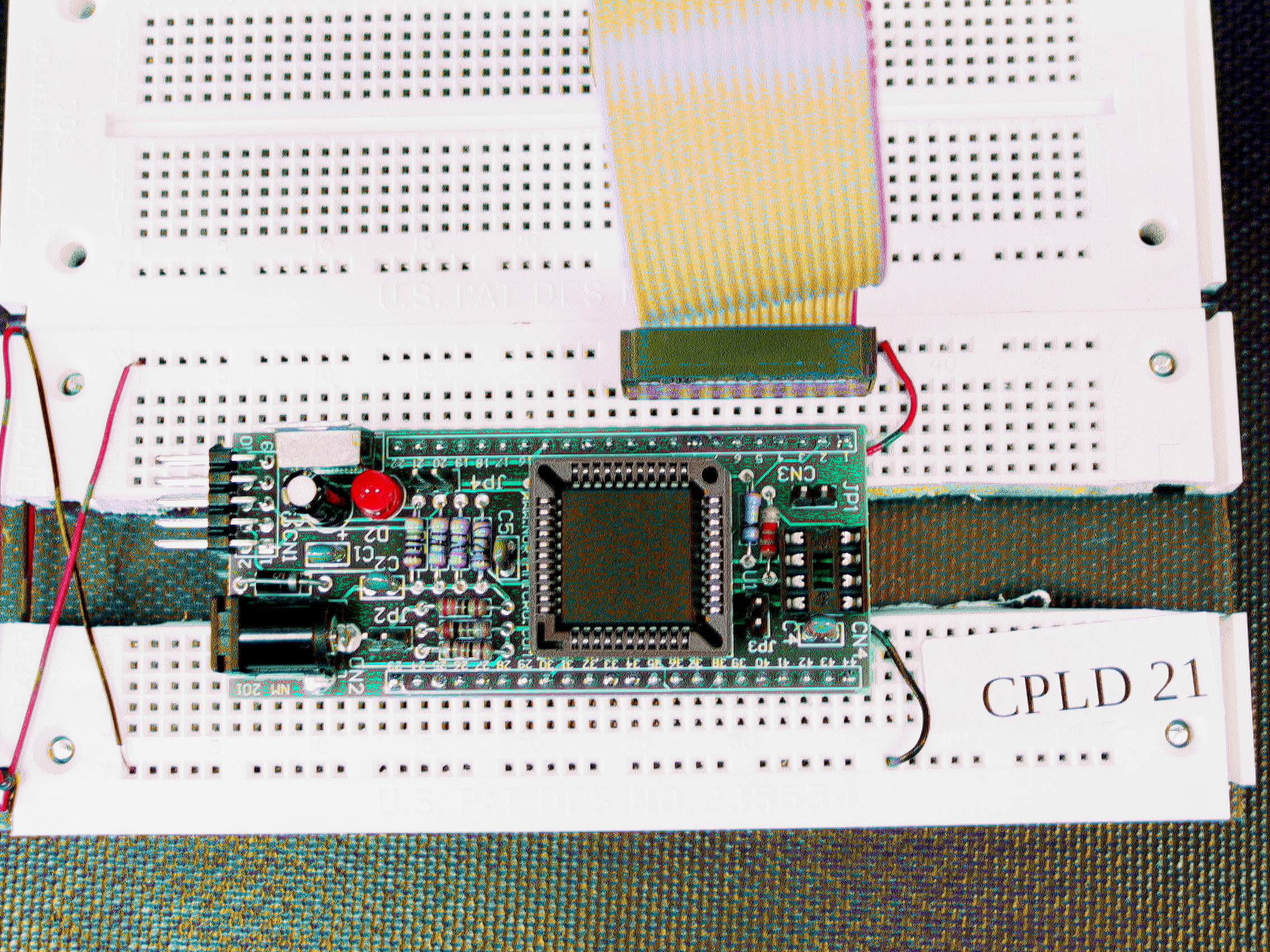
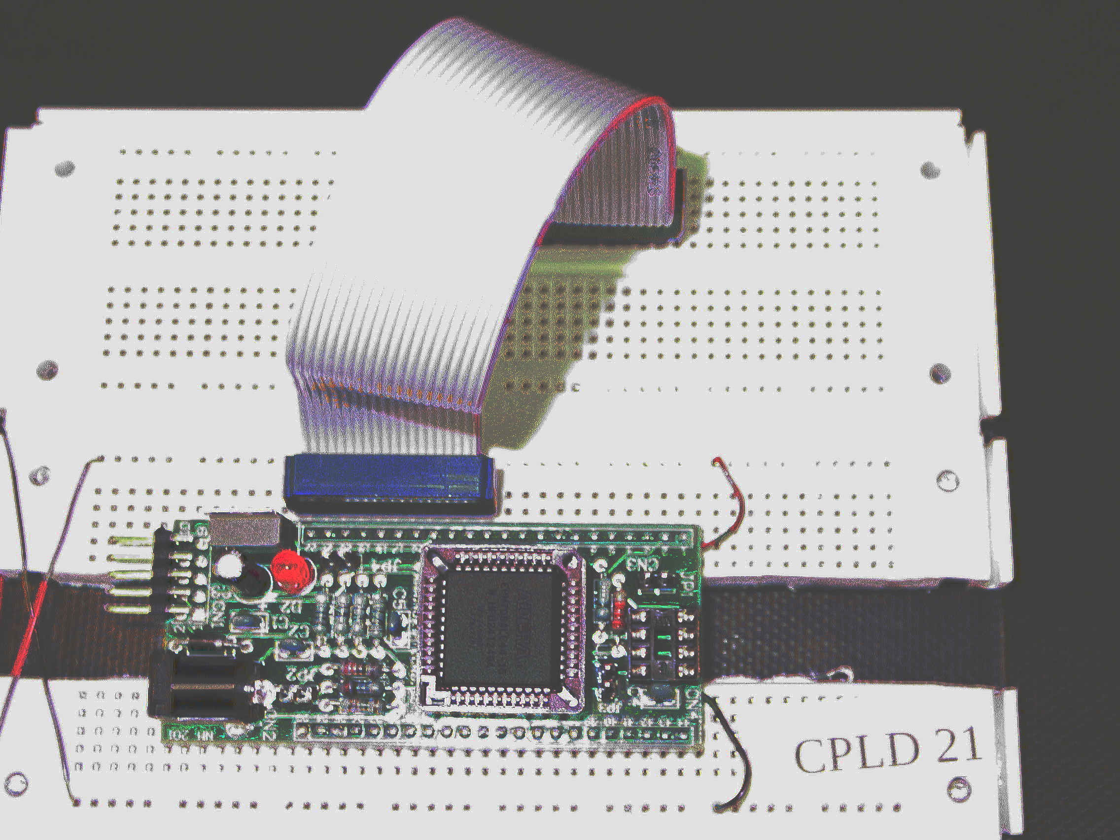
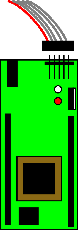
The other style of CPLD board looks like this:
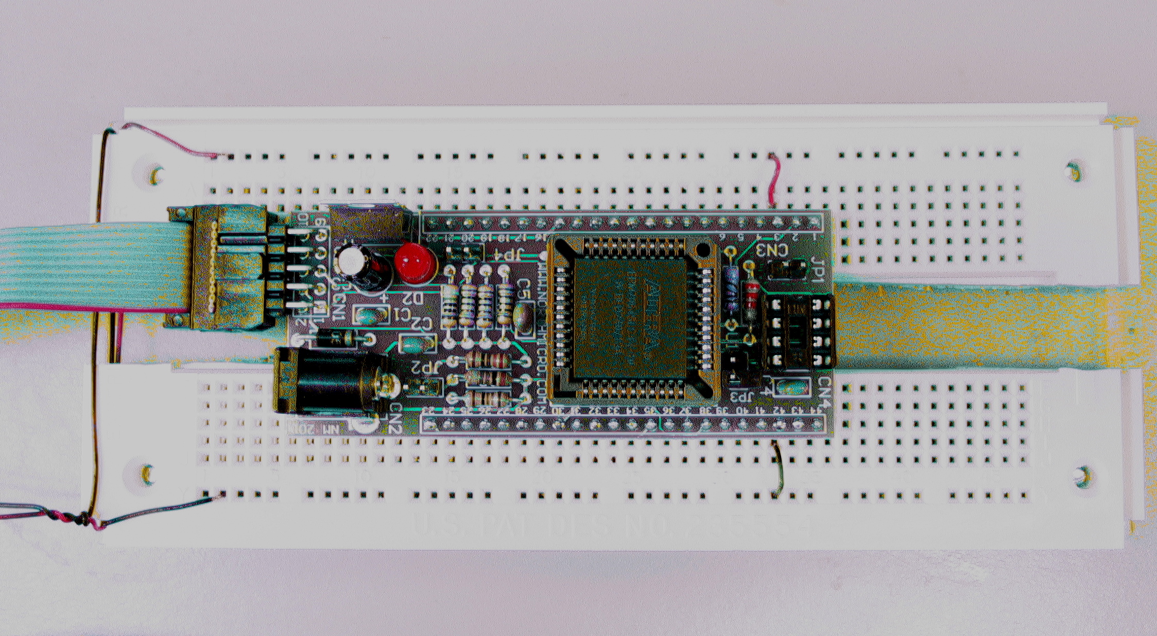
[click image to get a larger image]
Functionally the two types of boards are the same.
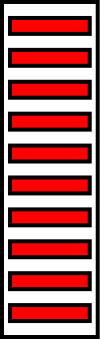
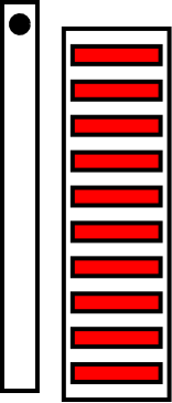
A
bargraph LED
is a collection of LEDs arranged
side-by-side in a single device. It's a compact way to display several
bits at once.
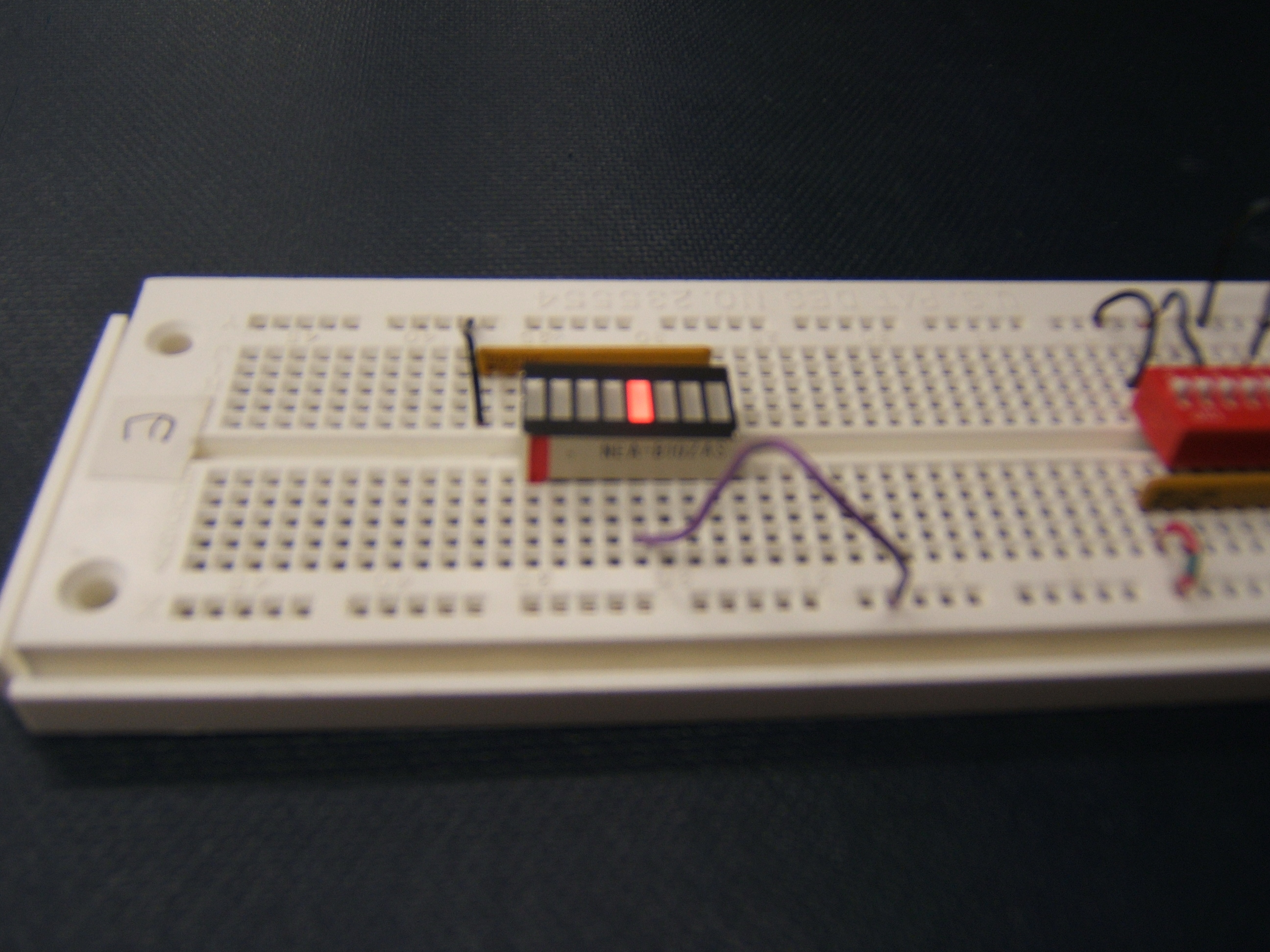
As with any LEDs, each one needs to be used with a resistor to limit
current. This can be done by putting an individual resistor in series
with each one. However, since they're all in a row, it's much easier to
use a resistor array instead.
If the common pin of the resistor array is grounded, then a high on the
other side of any LED should light it up, provided the LED is the
right way around. If you're not sure which way the display should
go, just turn it around if it doesn't work one way.
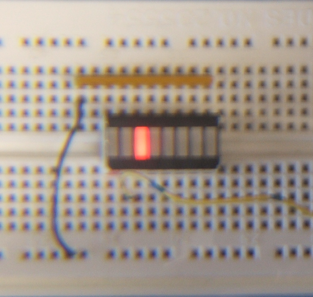
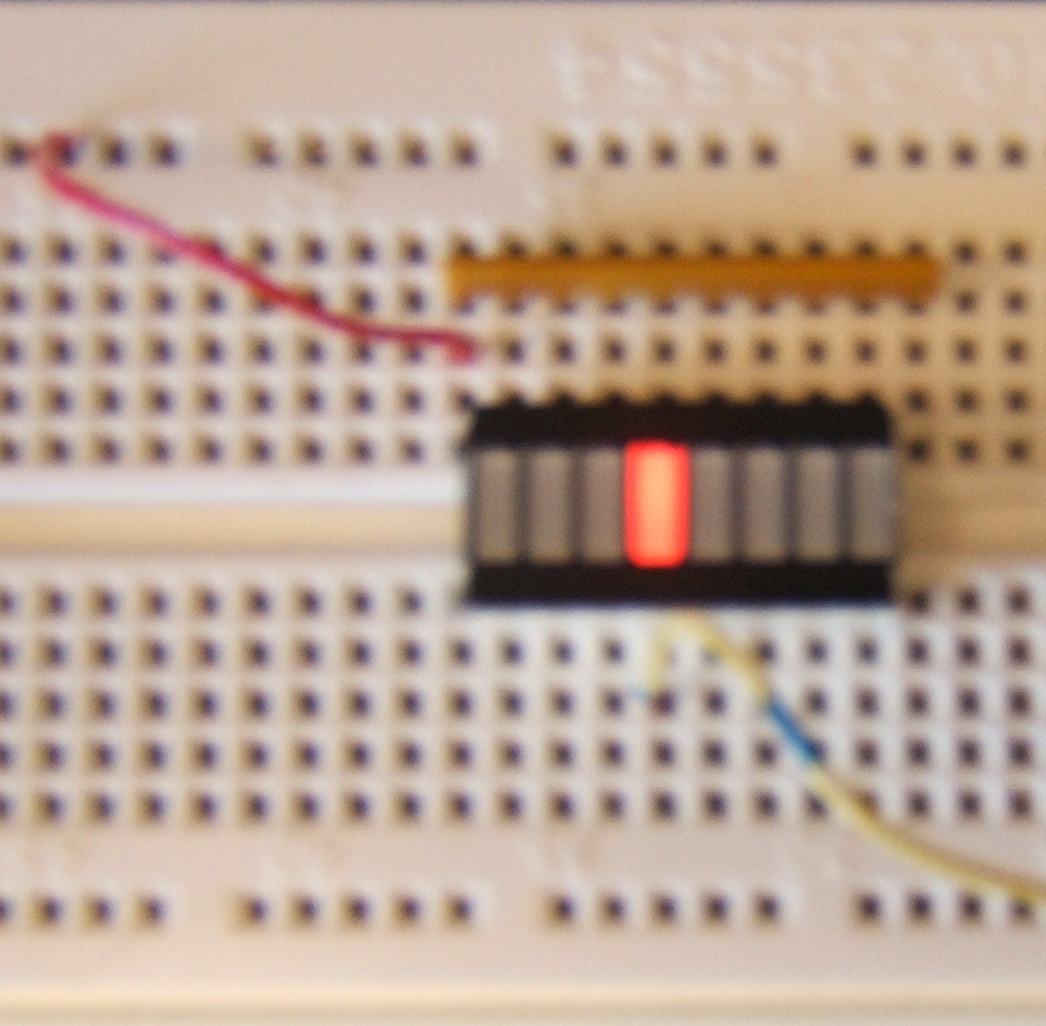
If you want a LOW (0) signal to light up the LED,
simply reverse the common connection and turn the bargraph display around.
(You need to turn the bargraph around since current will need to flow
in the opposite direction.)
The actual resistor value isn't critical;
anything between about 100 Ω and 1 k Ω should work. With
smaller values, the LED will be brighter; with larger values, it will be
dimmer.
Ideally you want to choose a large value that makes the LED bright
enough to see clearly.
The image below shows how the connections are the same as for an
individual LED. (The signals come in on the yellow wires.)
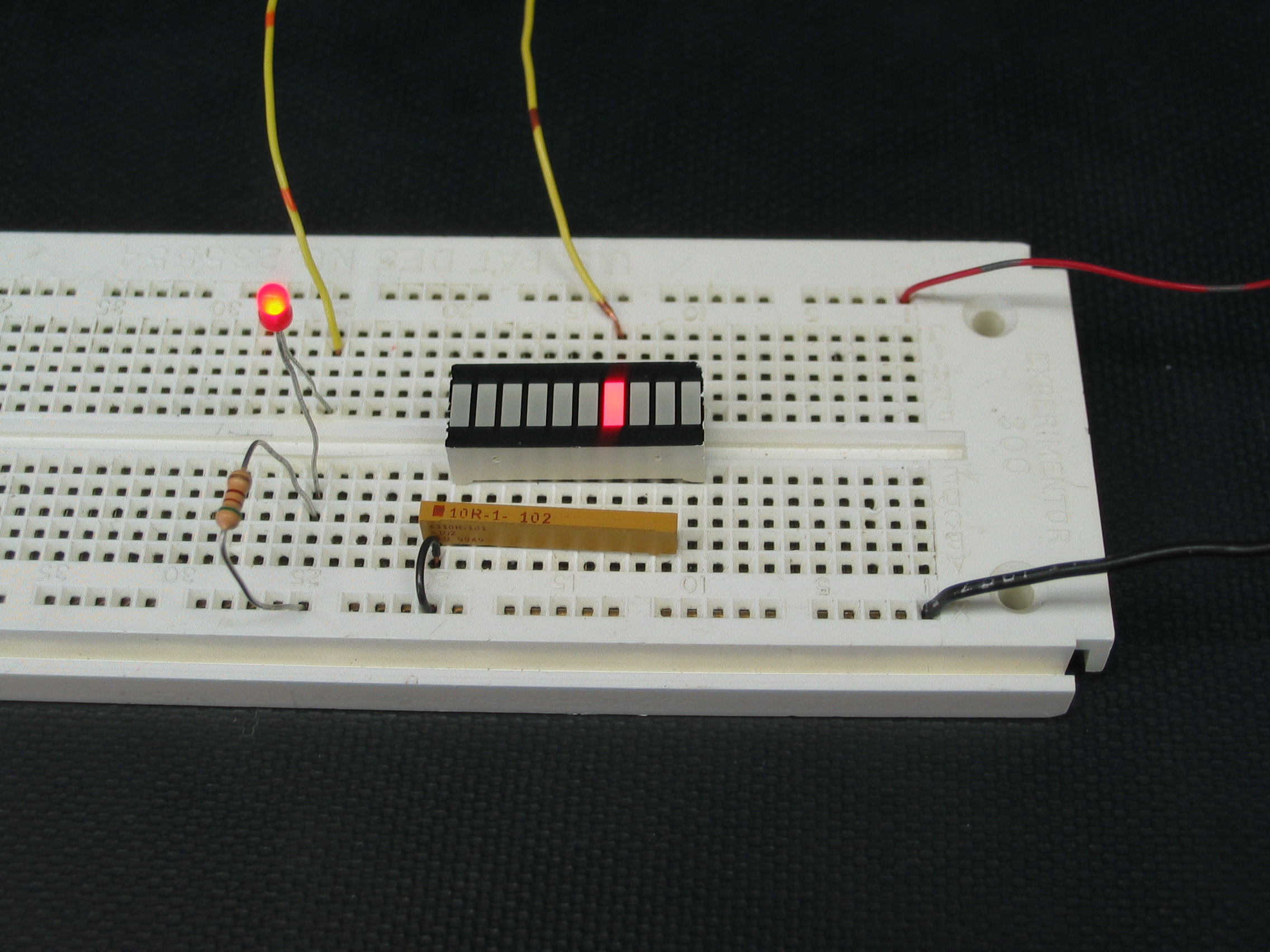
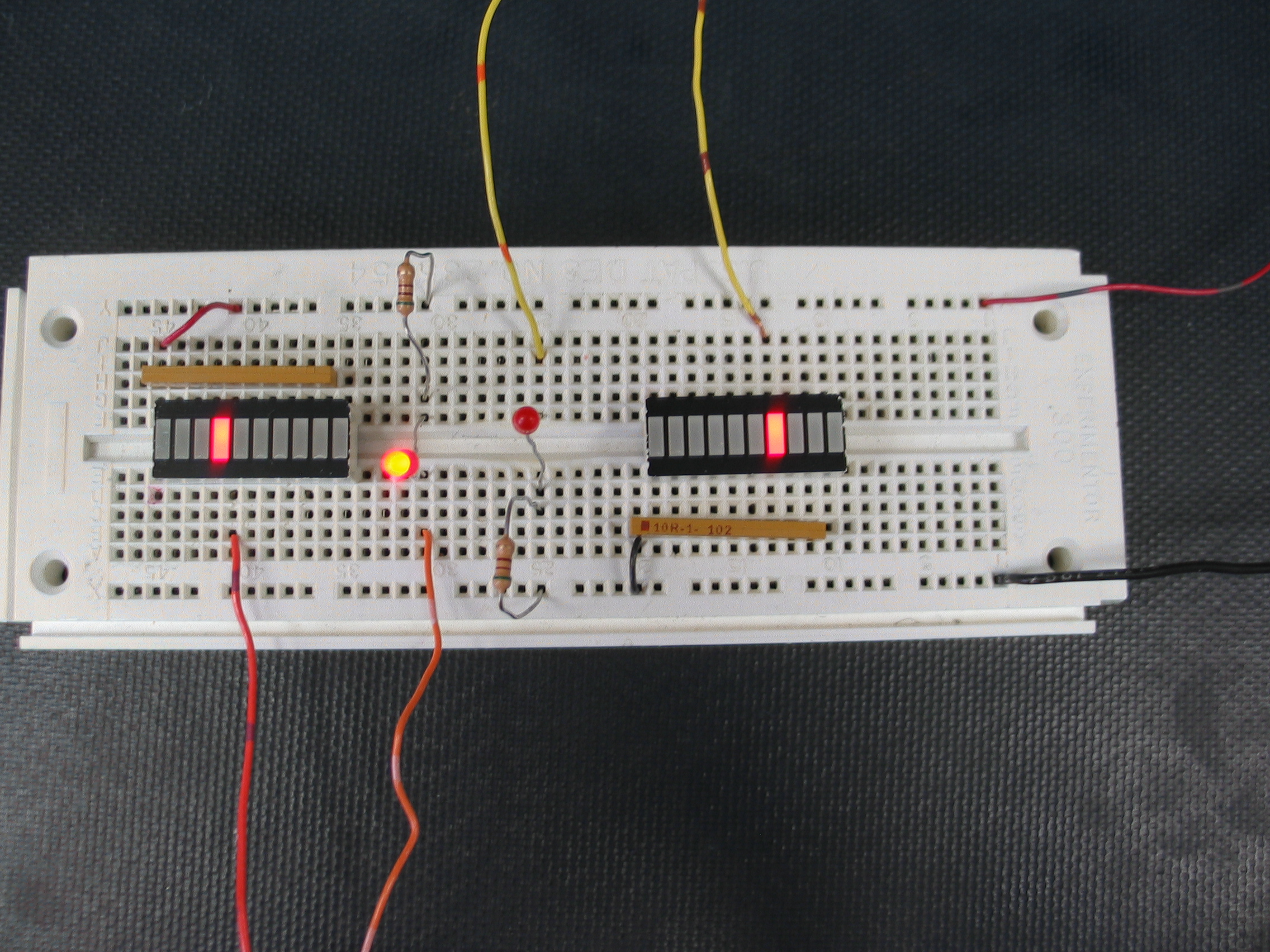
As wtih individual LEDs, they can be connected either active high or
active low. In the image below, the LED and bargraph on the right
are connected for active high signals, on the yellow
wires,
while the LED and bargraph on the left
are connected for active low signals, on the orange
wires.
(If you need a reminder of how to do this, go to the Quartus II introduction)
Create a new project called Myxor.
You'll be creating an exclusive or from AND, OR, and NOT gates.
For two inputs, A and B, the XOR function is given by:
f = AB
+ AB
Draw the circuit and compile it.
For the device, choose the EPM7064SLC44-10 from the
MAX7000S Family as before,
which is the device we are using in our lab.
(Remember to work on the E: drive, not the I: drive.)
Select Assignments | Pin Planner from the pull-down menu.
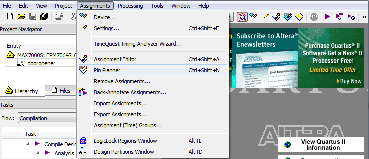
You'll see a schematic of your device which shows the status of various pins, with a list of your inputs and outputs below.
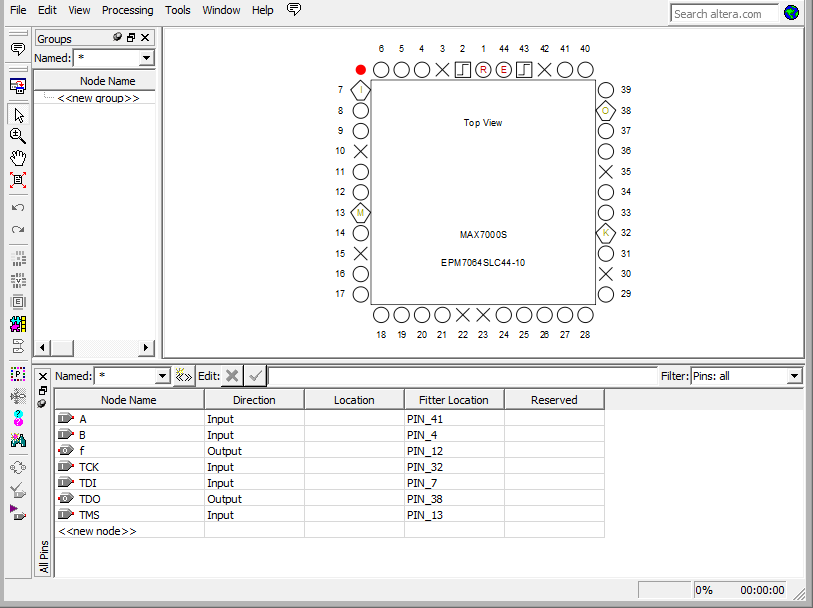
You will notice that the pins around the edges of the chip have different symbols. The plain round circles with nothing written inside of them are used for input and output.
Assign all of your pins to fit in one "bank" of CPLD connections, so only one jumper cable is required. Banks are:
For example, here is bank one.
One style of CPLD board looks like this:
[click image to get a larger image]
The other style of CPLD board looks like this:
[click image to get a larger image]
Here is bank two.
One style of CPLD board looks like this:
[click image to get a larger image]
The other style of CPLD board looks like this:
[click image to get a larger image]
Select each input and output from the bottom of the screen and
drag it on top of the pin you would like to use - make sure you click on
the name. (ie. if you want A to be pin 4, click A on the bottom of the
screen and drag it on top of the circle under the label 4).
Remember, use ONLY the plain round circles!!
You only need to assign your inputs and
outputs;
you will probably see some other signals listed that you didn't specify.
Leave them as they are.
When you are finished you can close the window.
You will need to compile your design again to fit your design on the PLD board.
Click on Processing | Start Compilation to start compilation.
Connect your USB-Blaster cable to one of the USB ports on your computer.
Choose Tools | Programmer. The Programmer window will open.
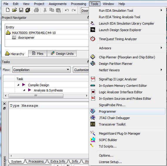
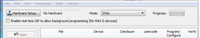
The selected programming hardware is identified as. If it says "USB-Blaster [USB-0] mode JTAG" you have the correct hardware (skip to connecting programming hardware to the device).
Click the Hardware Setup button to open the Hardware Setup window.
Programming hardware that is already set up appears in the Available hardware items window.
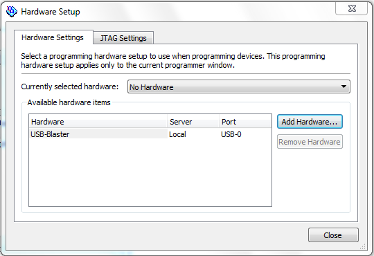
If the USB-Blaster is not listed as the Currently selected hardware, select it and click the Add Hardware.
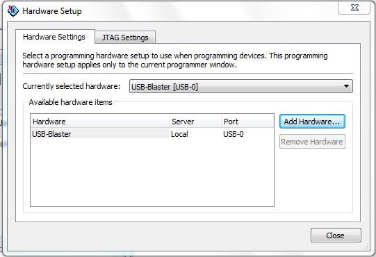
Click Close.
At the main window, ensure it displays USB-Blaster[USB-0] mode JTAG (see figure below)
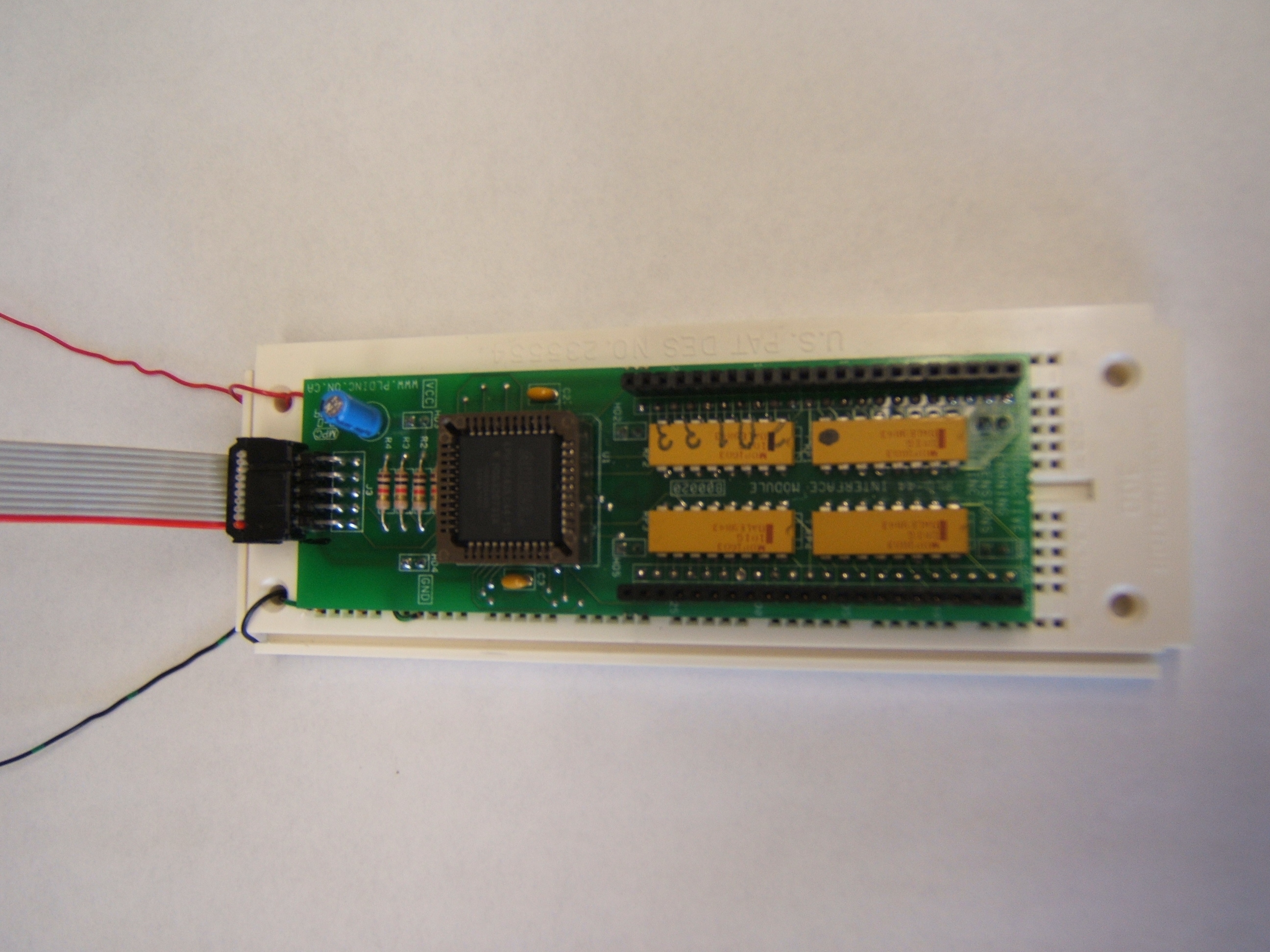
Connect CPLD board to USB-Blaster cable (connected to a USB port on
your PC).
One style of CPLD board looks like this:
The cable should be attached so that the red edge of the USB-Blaster
cable is next to the number (usually a "1" or a "2") that has been
written on the board with a marker. IF YOU'RE NOT SURE, ASK!!!
The other style of CPLD board looks like this:
The cable should be attached so that the red edge of the USB-Blaster
cable is away from the edge of the board as shown below.
IF YOU'RE NOT SURE, ASK!!!
[click image to get a larger image]
[click image to get a larger image]
Connect the ground and power (5v) to the CPLD board and turn the power on.
Click Auto Detect, and Quartus II
should detect the CPLD.
If it doesn't, there are three possibilities:
| Problem | Solution |
|---|---|
| Unable to scan device chain. | This is generally a problem with power. Check:
|
| JTAG error | This is generally a problem with the connection. Try:
|
| License error | This is generally a problem if you haven't done anything with the software recently. The server times out and loses the connection to the licensing file.
|
Once it autodetects correctly, you can proceed.
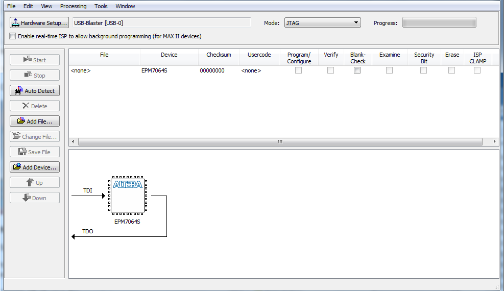
Delete the file that shows up.
Click Add File choose 'pof' file
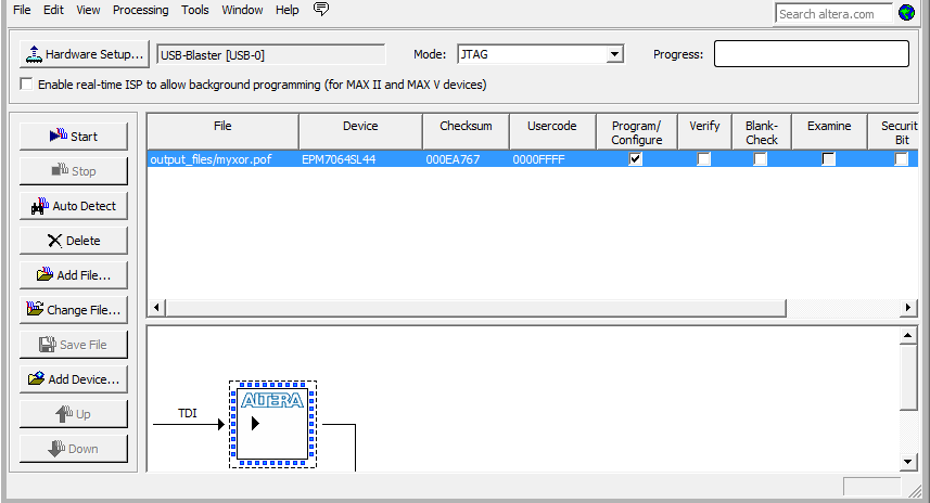
Check Program/Configure
Select Start, you should see the progress indicator increasing. (If it instantly jumps to 100% it indicates a problem.)
You can unplug the USB-Blaster cable and turn off the power while you are wiring your circuit. You will not lose your program.
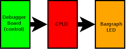
Use the debugger board to wire the input (use control mode) and a bargraph LED display for the output. If you want, you can display the inputs on the bargraph display as well.
Be sure to
daisy-chain
the breadboard(s) and the debugger board,
rather than using several clip leads or having clip leads holding more
than one wire.
You may want to use the debugger board for output to see that the CPLD
is working, and then
wire up the bargraph display once you know it should be getting the
correct signals.
This is another example of modular design.
If you smell smoke turn off the power immediately and DO NOT touch the Altera chip. It gets extremely hot if it is short circuited. Check all your power and grounds, have someone else check your power and grounds - something IS wrong!! Hopefully, your chip will still work. :)
Demonstrate the circuit to the lab demonstrator before you leave.
Delete everything from the E: drive so your files don't get used by someone else later.


![]()
Wilfrid Laurier University
© 2019 Wilfrid Laurier University