CP316: Microprocessor Systems and Interfacing
Introduction to the Development Environment
(Debugger)
Objectives
When learning a new microprocessor or microcontroller, especially one with a
Harvard architecture like the PIC, it is important to understand how the memory
address space is structured. For microprocessors with a Harvard architecture,
the data and program memory may have completely different structures.
It is also
important to determine how the IDE can be used to view memory and how the IDE
will respond when you access nonexistent memory.
- understanding program memory addresses
- understanding data memory addresses
- introduce additional functions of the MPLABX IDE
- introduce use of the MPLABX IDE debugger
- understanding the operation of the banked memory
Equipment
Procedure
NOTE: Some groups may find this lab long. Any material not
completed in the lab is homework.
The MPLABX debugger allows you to run code on the
target board, while still being able to single step, use breakpoints,
and examine memory.
- Watch this
video on viewing memory in MPLABX. (It's about 6 minutes
long.)
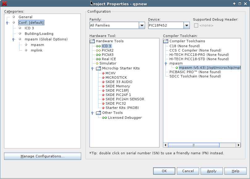
First, you need to access project properties:
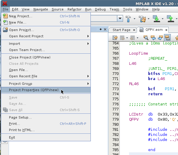
To choose the debugger or programmer, you need to choose the ICD3
instead of the
simulator in the project properties:
(Note: If the debugger is already running, it must be
stopped in order to allow access to
project properties.)
To simplify using watch windows, you need to
set to build in absolute mode.
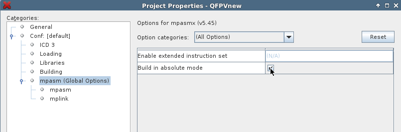
After this, you should be able to use variable names when setting
watches.
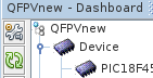
Instead of using the menu, you can access project propertties using
the wrench icon on the dashboard.
- The PIC18F452 has 32 Kbytes of Flash program memory,
where
K is 1024. How many bytes (in decimal) are contained in the Flash program
memory?
- Program memory is byte addressable which means every byte has
an address. If the lowest address is H'0', what is the highest address (in
hex) in the Flash memory? Show your calculations.
- How many bits are required to represent this address range, i.e. how many
bits are required to store the highest address? How does
this number compare
to the width of the instruction address bus as presented in Figure 1.3 on
page 13 of the text?
- The PIC18F452 has the potential for addressing 2 Mbytes of program memory
space with its 21-bit program counter. Not all models of the PIC18 family
have the full 2Mbytes implemented on the microcontroller.
Note that unimplemented
program memory is always at the end of the program memory address space.
If you access a nonexistent memory location between the
physically implemented
memory and the 2 Mbytes maximum, the processor will cause
a read of all ’0’s
(a NOP instruction).
How much program memory does the MPLABX IDE let you view? Open the
IDE, and look at program memory in hex.
(Make sure you have
the correct device selected under configuration. A program doesn't have to
be loaded.) Does this match the implemented (32Kbytes) or the theoretical
(2Mbytes) program memory range?
- The data memory is implemented as
byte addressable static
RAM. If each location in the data memory has a 12-bit address, and all bits
are used, what is the lowest and highest address (in binary and in hex)?
How many locations (in decimal and in Kbytes) are in data memory?
- The implemented data memory is less than the theoretical data memory.
Unlike
the program memory the unimplemented portion of the data memory space is
in the middle of the address range. In the IDE,
open a memory view of file registers
and
scroll through the address space to find the large gap of
unimplemented memory.
Note the valid address ranges disregarding the small gaps
in high memory.
Look at Figure 4-7 from the datasheet. Note what it
says about "unused" memory.
- The lower chunk of data memory corresponds to
General Purpose Registers
(GPR) which is the general data area for the microcontroller.
Show that this chunk corresponds to 1.5 Kbytes. In general,
the GPR space
starts at location H'000' and grows up in memory.
- The significantly smaller upper chunk of data memory corresponds to
Special
Function Registers (SFR) and these are used to control and get
the status of the controller and peripheral functions. In general , the
SFR space starts at location H'0FFF' and grows down in memory.
In the IDE,
if you view the file registers using the Symbolic option, you
will notice the SFRs have predefined names. This area can also be viewed
by selecting
a view of special function registers
in the IDE.
Demonstration - explain the program and data memory layouts;
explain how
you can view these areas in the IDE.
- Set up a test project that contains your version of test.asm from
the last lab. Assemble the program and open a window containing
the listing
file, test.lst. View program memory using symbolic mode.
You should see the correspondence between the listing file and the contents
of program memory. How does the display change if
you select the
or the hex option to view program memory?
- In the listing file, find the following lines of code:
000018             org        0x0018        ;low priority interrupt vector
000018 EF0C F000   goto       $             ; ... tight loop for now
Find the corresponding location in the program memory. What was the goto
$ translated into?
The "$" sign is a special character and it represents the
address
of the present instruction. In this section of code it is used to create
a tight loop. If, by some chance, a low priority interrupt occurred, the
program would go into a tight infinite loop. The program does not expect
any interrupts and is using this section of code as a place holder.
- Switch to the file register view. Remember
this is data memory and locations 0x0000 to 0x0002 should correspond
to num1, num2,
and result.
Notice that under the symbolic option these locations
are called A, AN1, and AN2.
Since we didn't define
these labels, they must be coming from the "include" file.
Look
at the symbol table at the end of the listing file. Did the include file
labels overwrite our labels or do these memory locations
have multiple labels?
Does the file register view show the first label to be defined
for a memory
location or does it show the label that would be first
if sorted alphabetically?
Modify the program and test your hypothesis.
- What happens to the file register view if you comment out the include and
the configuration lines? Note that if you only comment out the include, the
configuration definitions will not work as they depend on labels defined
in the include.
Demonstration - explain the program memory view and the file
register view.
- Go back to your version of test.asm from the last lab and rebuild.
Launch the debugger, and
ready the program for execution by selecting reset
Note where the execution cursor position
is located. Explain.
- Now single step through the program using the step into button.
While stepping through the program notice the execution cursor
position and
the contents of the
status line
at
the top of the screen.
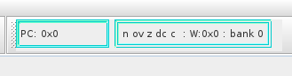
- What does the status register contain at the
start of the program?
- What does the status register contain after completion
of the add?
- Does the current program counter contain the value of
the line currently
being executed or the next line to be executed? How can you tell?
- Note the contents of the W register as you
step through the program.
- Reset. Open a program memory view (symbolic) and
a file register view (symbolic).
Within the debugger,
clear the file registers.
(You can right click in a data memory view and Fill
memory with zeros.)
Now single
step through the program.
- It is simple enough with only three variables to
mentally map between our
labeling and the system's labeling in the file register view.
However, with
more variables, it is more efficient to set up a watch window
(see the Quick
Start Guide). Set up a watch window with our three variables (from symbols)
and wreg (from SFR). Clear the file registers.
Single step through the program.
Did you notice the address of wreg? What does this mean?
Demonstration - demonstrate the use of a watch window
and explain the
location of wreg.
- Data memory doesn't quite work like typical linear memory.
Change the cblock
address to 0x080. Using the watch window as your debugging tool,
single step
the program. Other than the movement of the data to a different location
in memory, the program should work as you would expect.
- Change the cblock address to 0x100. Using the watch
window as your debugging
tool, single step the program. The program does not appear to work.
- Open the file register view and the program memory view as well as the
watch window. Clear the file registers. Single step the program. Does the
program work? Where does the data appear to be located?
- Memory is divided into banks containing locations 0x000 to 0x0ff.
The memory
bank select register, BSR, points to the bank number.
By default, BSR is
zero. Add the line
movlb 1 ;set memory bank
to the start of the main routine. Add BSR to the watch window.
Clear the file registers and single step the program.
Things should now look
OK. The movlb instruction moves the literal,
in this case "1",
to the bank select register.
- Test the following combinations, making sure to clear the file registers
before executing, and use the file register view to determine the location
of the data memory being updated. Open the program memory view. You do not
have to single step the program; simply run the program and stop it when
it goes into the last tight loop. What can you deduce
from this exercise?
| cblock |
bsr |
Location of num1, num2,
result according
to watch window |
Memory locations actually being
updated |
| 0x0000 |
0 |
|
|
| 0x0000 |
1 |
|
|
| 0x0000 |
2 |
|
|
| 0x0100 |
0 |
|
|
| 0x0100 |
1 |
|
|
| 0x0100 |
2 |
|
|
| 0x0200 |
0 |
|
|
| 0x0200 |
1 |
|
|
| 0x0200 |
2 |
|
|
Demonstration - explain the rules governing the bank
selection register.
Wilfrid Laurier University
© 2019 Wilfrid Laurier University


