Pages created and updated by
Terry Sturtevant
Date Posted:
May 12, 2017
In this tutorial, we will show you how you capture the schematic design for the automatic door opener circuit using Altera Quartus II software.
We are designing a circuit for an automatic door like those you see at supermarkets. The door should open only when a person is detected walking through or when a person presses a switch (such as the wheelchair button) to have the door open. The door should only operate if it has been unlocked.
During Labs you will need to save all your work under a directory called CP120 in your Home Directory (drive I:)
To get to your I: or your Home Directory double click on My Computer icon on the desktop.
Under I:\CP120 create the following folders
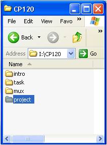
Copy this directory from the I drive to the E drive. There are currently problems saving files directly to the I drive. Be sure to copy your files back to the I drive after you are done.
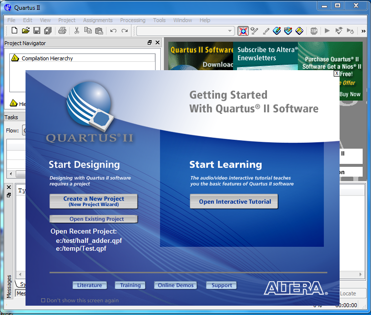
Launch the Altera Quartus software. You should see a screen such as this:
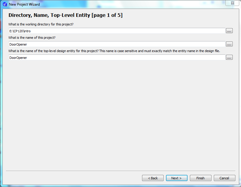
Select the File → New Project Wizard; a window like the following will appear.
To select the working directory use the button to browse and
select
E:\CP120\intro.
Name the project DoorOpener.
(Note that the next field gets filled in automatically.)
Select
Finish.
Don't uses spaces in file or directory names.
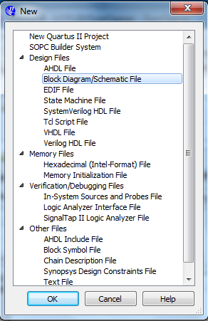
Select File → New - A window as seen in the following picture will open.
Select 'Block Diagram/Schematic File' and press OK.
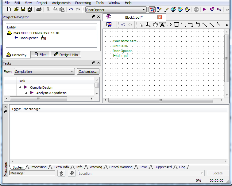
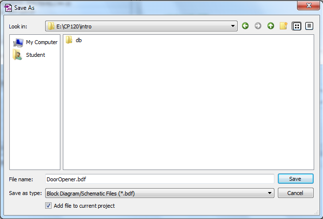
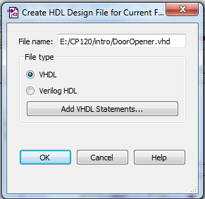
This should open a pane where you will design your circuit. This pane is designated Block1.bdf. Save this graphic design file as DoorOpener in your "intro" directory. The file will be given the bdf extension; bdf stands for block design file and contains schematics, symbols or block diagrams.
![]()
Repeat these steps to enter an OR (or2) gate and a NOT (not) gate.
(If you wanted to add multiple NOT gates, you could select the Repeat-insert mode box.)
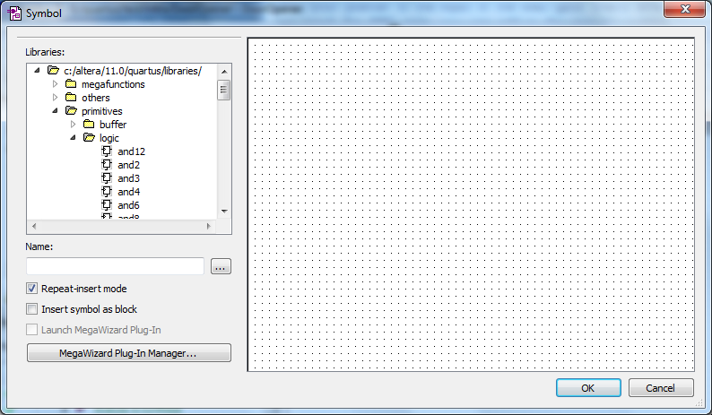
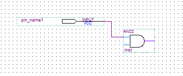
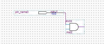
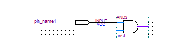
In the same manner that you placed a gate onto the palette, add three input pins and one output pin from the Symbol libraries. Input pins can be found under primitives | pin | inputs. Output pins can be found under primitives | pin | outputs.
Name your input and output pins as you name them in your equation. Double
click on the pin name to change its name.
Never use spaces in pin names; e.g. "input 1" is a problem - "input1"
and "input_1" are ok.
Rearrange your devices in approximately the placement you would like for the logic diagram you are trying to construct. You can move a component by selecting it with your mouse, holding down the left button and moving it to another location on the palette.
Save your design. It is a good
idea to save your design often, just in case something bad happens .
Save the bdf file with the same name as the project.
Don't use spaces in any file names.
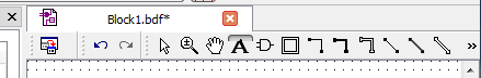
Select the orthogonal node tool. ![]() Place your pointer on the output of one of the input pins and
hold the
left mouse button down. You should see a cross-hairs or + appear at the
output.
Place your pointer on the output of one of the input pins and
hold the
left mouse button down. You should see a cross-hairs or + appear at the
output.
Drag your pointer to the input of the AND gate. Every time you release the
mouse key, the line (wire) ends. If your wire did not reach the AND gate, you
can add to the wire by putting your mouse over an end of the wire and again
selecting it with your left mouse button and dragging your mouse to another
position.
Don't run wires along the edge of a device. This
can cause simulation problems.
Don't leave inputs and outputs right next to the
chips. Make sure you can actually see some wire between them, otherwise
you may have simulation problems.
Note: Make sure you do not make the wire too long. If you drag it too far you will see an x; and this is considered an open connection and your design will not compile.
To delete a wire or a portion of a wire, simply click on it (it should change color to indicate selection) and press the delete key.
If wires are connected to the component as you are moving it, the wires will
drag and stay connected to the component. This is referred to as "rubber
banding" and is a feature of all major schematic entry design packages.
(You can turn rubberbanding on and off using the rubberbanding tool.![]() )Add the
rest of the wires needed to connect the logic diagram.
)Add the
rest of the wires needed to connect the logic diagram.
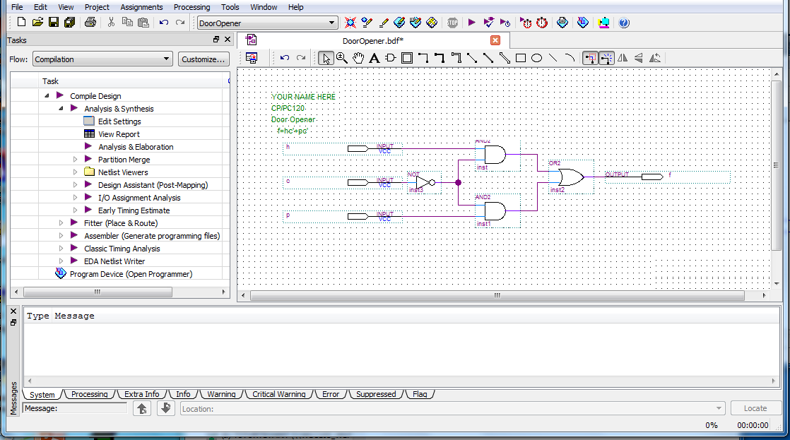
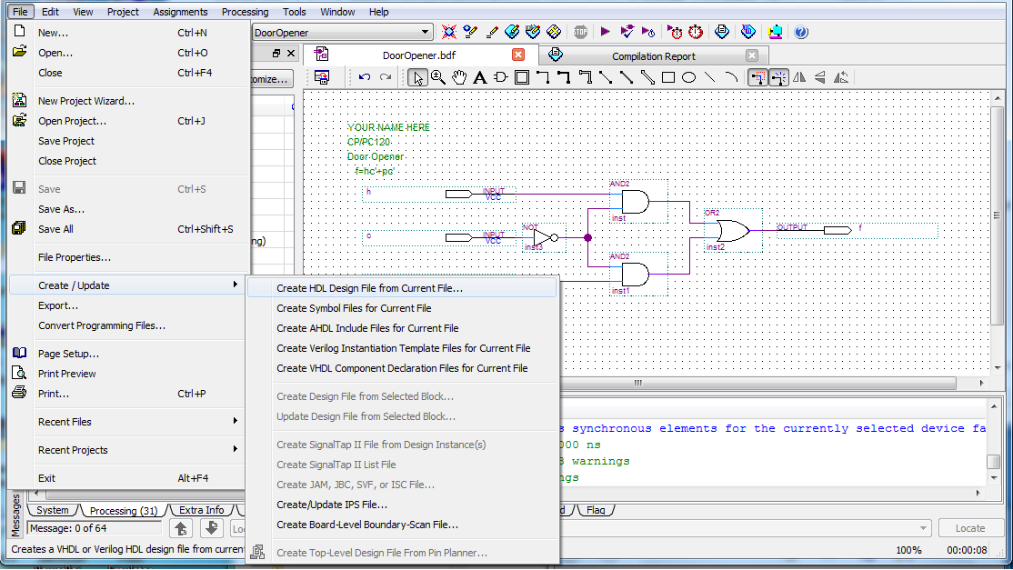
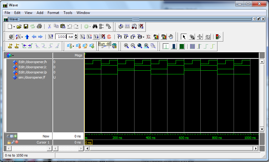
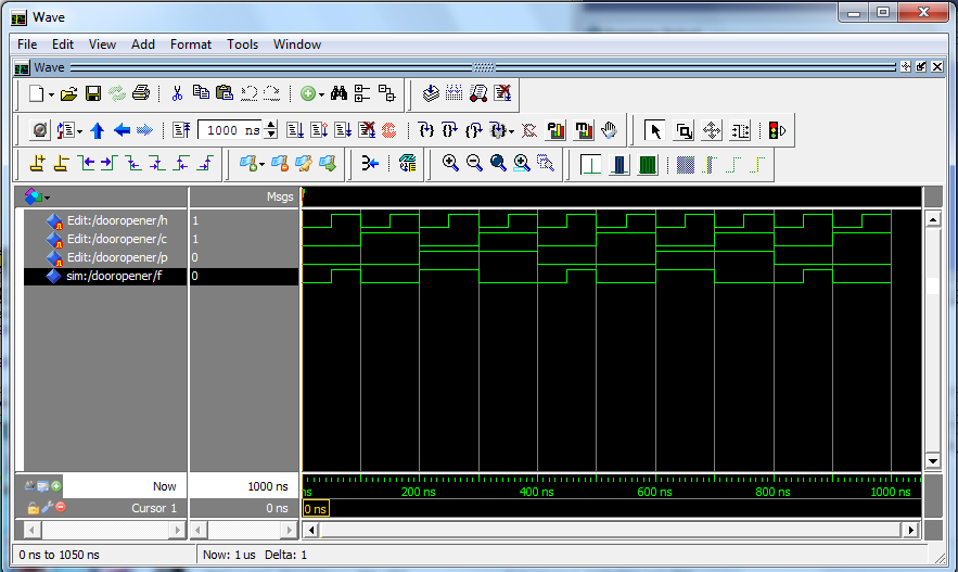
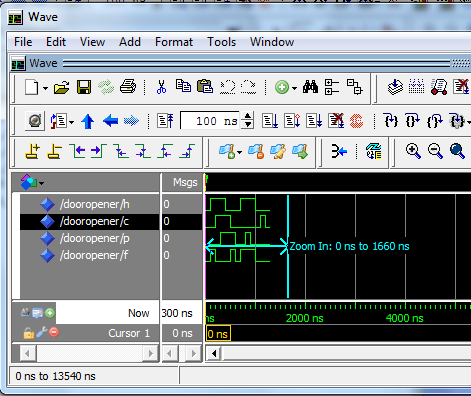
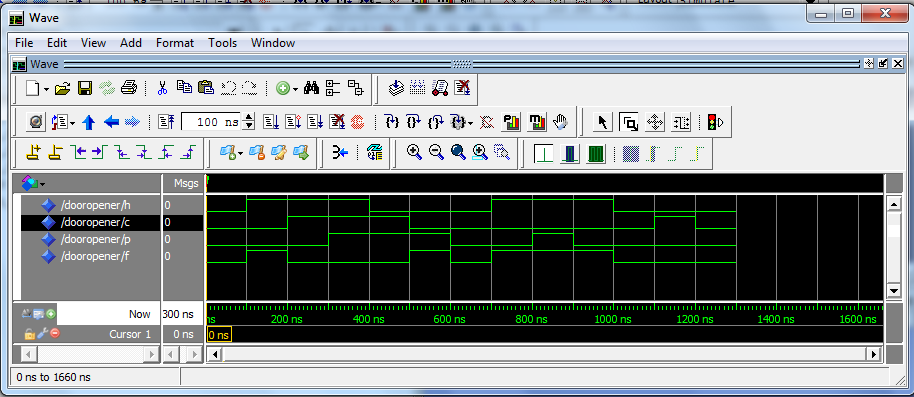
The window should look something like image below. Save your design.
We will not print today. But you will need to know how for your project.
To print, go to File | Print. If you want to change what appears on the printout or how it appears, go to File | Page Setup change print settings. Before printing, you can view what the print will look like by selecting File | Print Preview
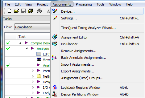
The programmable device which we'll use for our design can be chosen now.
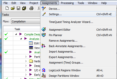
Select Assignments | Device from the pull-down menu.
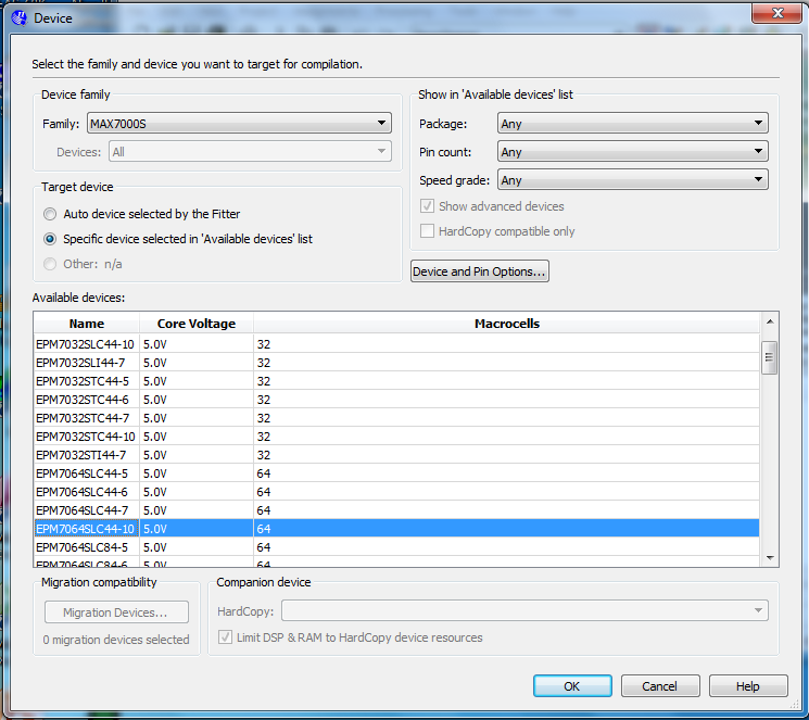
Select MAX7000S from the "Family" pull-down list. Select the "Specific device selected" and then choose EPM7064SLC44-10, which is the device we are using in our lab. Select "OK."
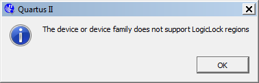
If you get a message like this, don't worry; it's fine.
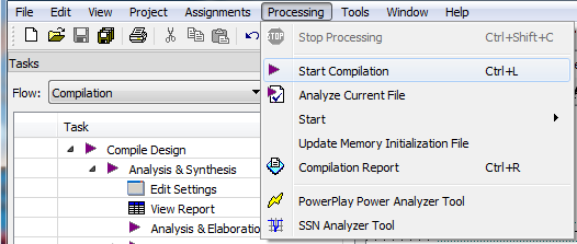
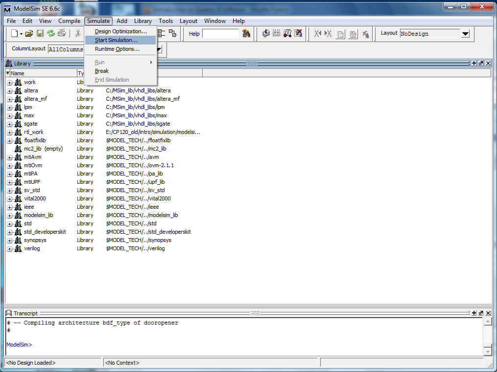
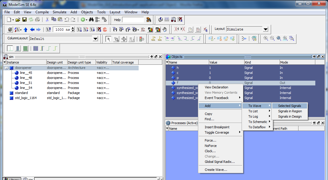
You will need to compile your design to ensure you do not have any errors in your circuit (e.g. you do not have any open connections, etc.)
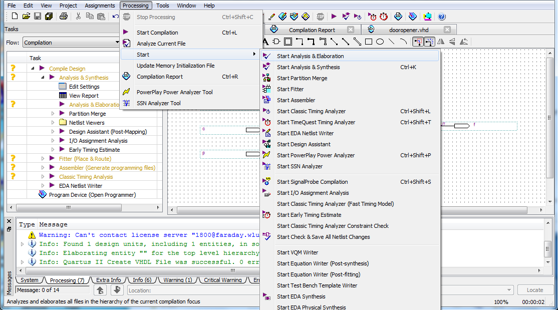
Click on Processing | Start Compilation to start compilation.
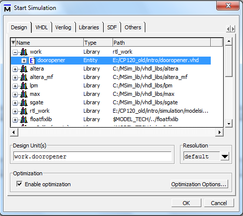
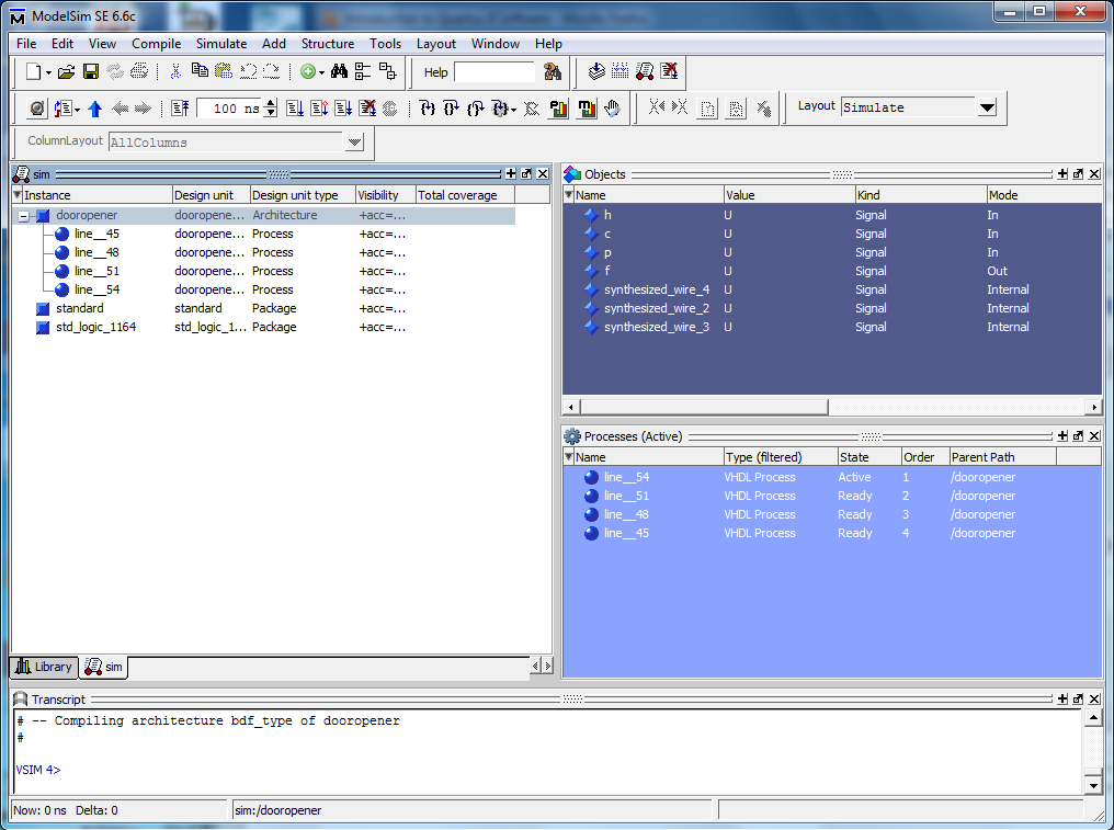
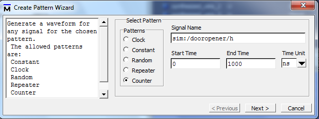
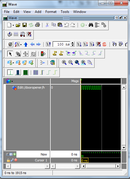
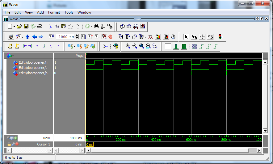
Before simulating, some preparation is required.
It may be necessary to compile the libraries for your device family
before you simulate.
If you are using Modelsim-Altera, you will not need to do this.
All of the libraries are precompiled. If you are using Modelsim, you
may need to do this.
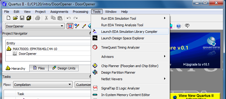
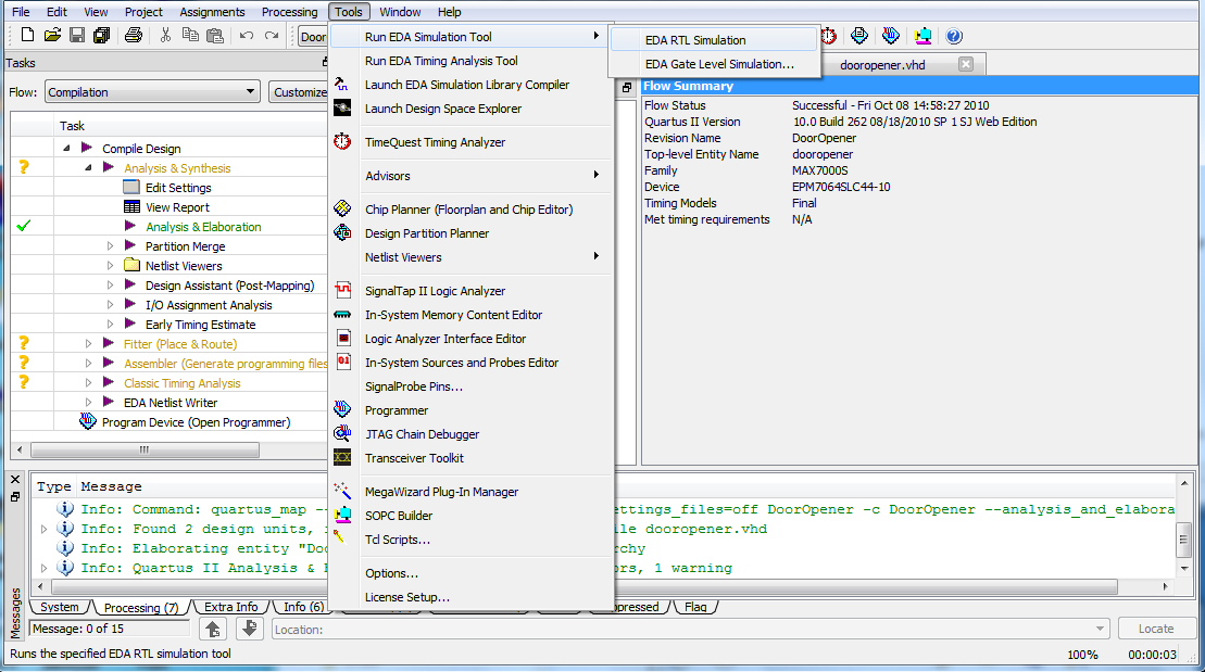
Click on Tools | Launch EDA Simulation Library Compiler.
The MAX7000S family should already be selected, so click Start Compilation.
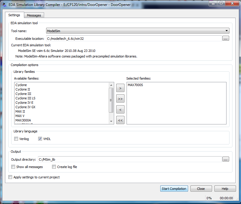
Don't worry if you get any error messages.


Wilfrid Laurier University
© 2019 Wilfrid Laurier University