Quartus II Tutorial
Introduction
Altera Quartus II is available for
Windows and Linux. The instructions here are from version 11.0, with
some updates for versions 12.0, 12.1 and 13.0. I try to keep it up to
date.
On my YouTube channnel, I have a
series of videos about Quartus II.
Using Quartus II
-
-
- Creating a New Schematic
- Adding Text
- Adding Components
- Wiring the Circuit
- Printing
- Choosing a Device
- Simulation
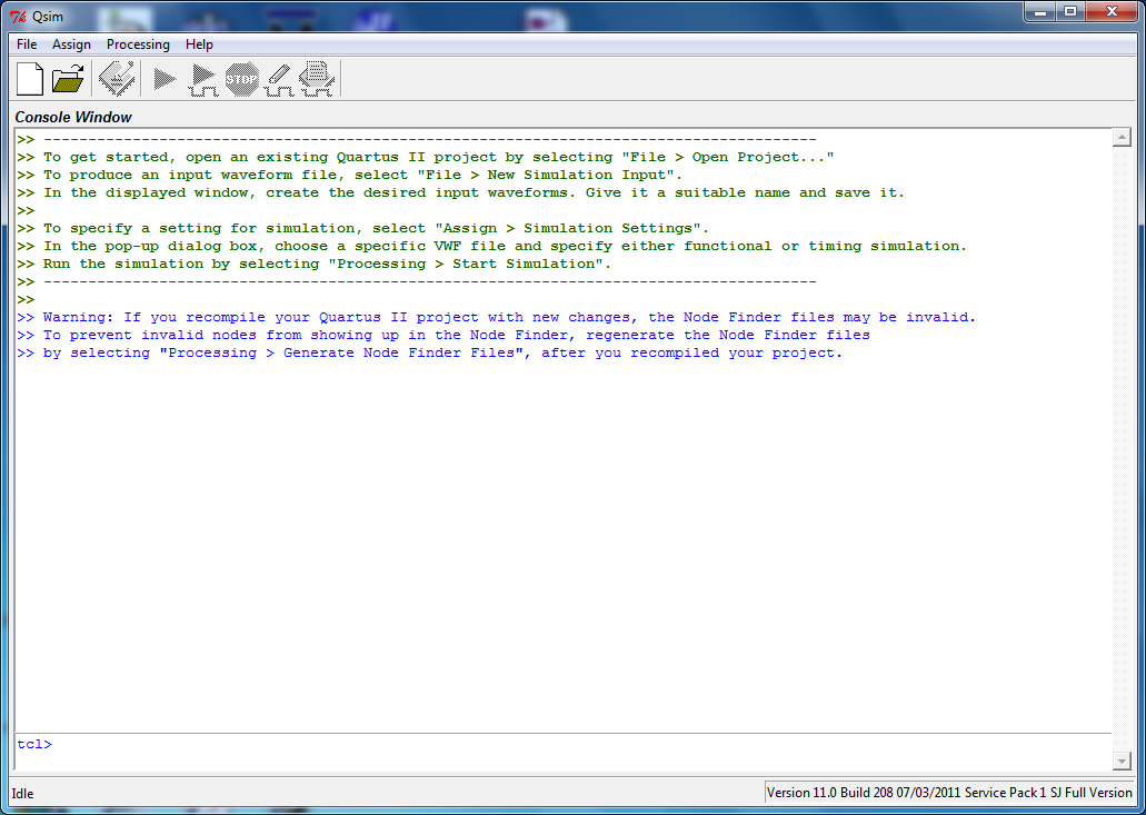
Note: Since version 11.1 of Quartus II, the QSim
simulator has been automatically included with Quartus II, for
Windows and Linux. For simple simulations, it is easy to use.
Following are instructions for simulations using either one.
- Preparing for the Simulation
- Methods of Simulation
- Forced Inputs
- Waveform Editor
- Testbenches
- Examining the Output
-
- Preparing Circuit for CPLD
- Assigning Pins
- Recompiling Design
- Selecting the Programmer
- Connecting to the Programmer
- Problems with the Programmer
- Wiring the Input and Output
- Troubleshooting
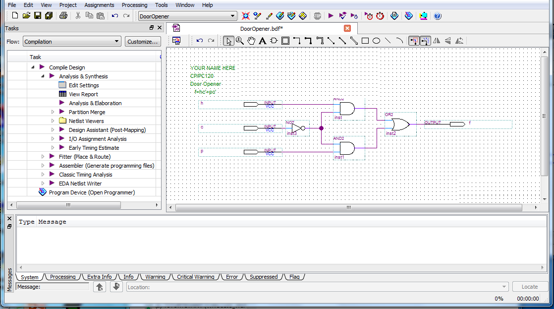
In this tutorial, we will show
you how you capture the schematic design for the automatic door opener circuit
using Altera Quartus II software.
The Problem
We are designing a circuit for an
automatic door like those you see at supermarkets. The door should
open only when a person is detected walking through or when a
person presses a switch (such as the wheelchair button) to have
the door open. The door should only operate if it has been unlocked.
- output: f = 1 (Opens Door)
-
inputs
- p = 1 Person Detected
- h = 1 Switch Holding the Door Open
- c = 1 Door Closed/Locked
- Want door to open when
- the door is unlocked and person walking through (c=0 and p=1)
- the door is unlocked and the switch is set to hold it open
(c=0 and h=1)
I: Drive
During Labs you will need to save all your work under a
directory called
CP120 in your Home Directory (drive I:)
To get to your I: or your Home Directory double click on My Computer icon on
the desktop.
Under I:\CP120 create the following folders
Copy this directory from the I drive to the E
drive. There are currently problems saving files directly to the I
drive. Be sure to copy your files back to the I drive after you are
done.
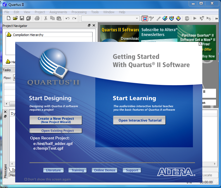
Getting Started with Altera Quartus
Launch the Altera Quartus software. You should see a screen such as
this:
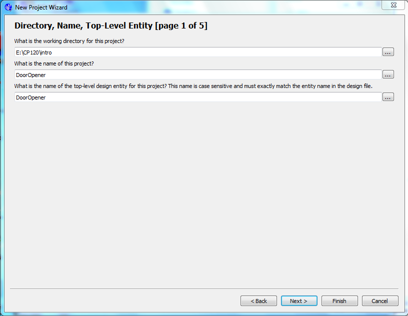
Creating a New project
Select the
File →
New Project Wizard; a window like the following will
appear.
To select the working directory use the button to browse and
select
E:\CP120\intro.
Name the project DoorOpener.
(Note that the next field gets filled in automatically.)
Select
Finish.
Don't uses spaces in file or directory names.
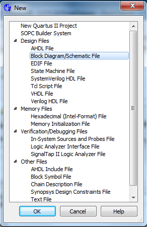
Creating a new Schematic design
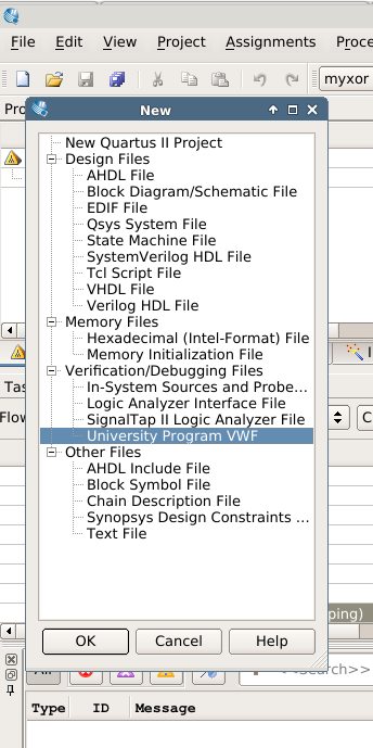
Select File
→ New -
A window as seen in the following picture will open.
Select 'Block Diagram/Schematic
File' and press OK.
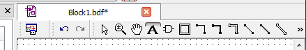
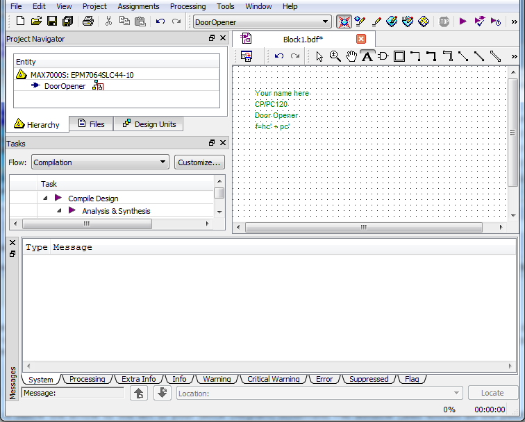
This should open a pane where
you
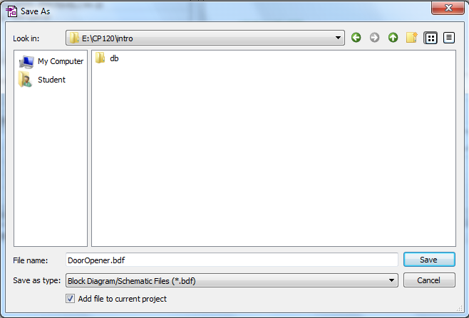
will design your circuit. This pane is designated Block1.bdf. Save this
graphic design file as DoorOpener in your "intro" directory. The file
will be
given the bdf extension; bdf stands for block design file and contains
schematics, symbols or block diagrams.
Adding text
- There is a toolbar on the
Block Diagram/Schematic File
drawing pane.
(This toolbar is also known as the
palette).
Select the A from the palette.
- Select a point near the top left in
the window with the left mouse key.
- Type your name and then hit the
Enter key.
- Type your project name and then hit
the Enter key.
- Type the following equation,
f = hc' +
pc'
, and then hit the Enter key.
- Hit the Esc (escape) key to end
text additions.
Adding a Component
- Click the
library icon from the palette.
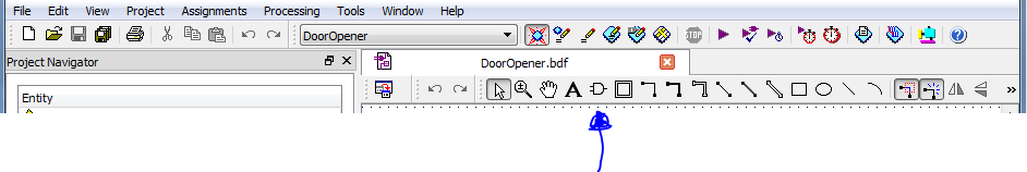
The Symbol dialog
box will appear. This window lists the available Altera libraries as seen
in this image.
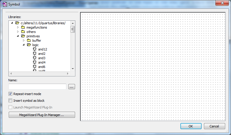
- Expand the
/altera/⟨current-version⟩/quartus/libraries
folder, expand the primitives folder and then expand the logic folder.
- In the logic folder, select the
and2 component by double clicking on it (or by selecting it with a single
click, then selecting OK).
- Click the pointer at the desired
location in the Block Diagram/Schematic Editor window to
insert the AND symbol
into the design file.
Repeat these steps to enter
an OR (or2)
gate and a NOT (not) gate.
(If you wanted to add multiple NOT
gates, you could select the Repeat-insert mode box.)
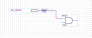
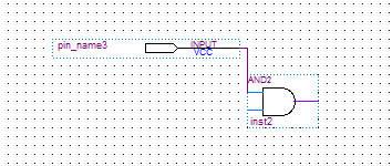
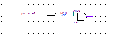
In the same manner that you placed a
gate onto the palette, add three input pins and one output pin from
the Symbol libraries. Input
pins can be found under primitives | pin | inputs. Output
pins can be found under primitives | pin | outputs.
Name your input and output pins as you name them in your equation. Double
click on the pin name to change its name.
Never use spaces in pin names; e.g. "input 1" is a problem - "input1"
and "input_1" are ok.
Rearrange your devices in approximately the placement you would like
for the
logic diagram you are trying to construct. You can move a component
by selecting
it with your mouse, holding down the left button and moving it to another
location on the palette.
Save your design. It is a good
idea to save your design often, just in case something bad happens .
Save the bdf file with the same name as the project.
Don't use spaces in any file names.
Wiring your circuit
Select the orthogonal node tool.  Place your pointer on the output of one of the input pins and
hold the
left mouse button down. You should see a cross-hairs or + appear at the
output.
Place your pointer on the output of one of the input pins and
hold the
left mouse button down. You should see a cross-hairs or + appear at the
output.
Drag your pointer to the input of the AND gate. Every time you release the
mouse key, the line (wire) ends. If your wire did not reach the AND gate, you
can add to the wire by putting your mouse over an end of the wire and again
selecting it with your left mouse button and dragging your mouse to another
position.
Don't run wires along the edge of a device. This
can cause simulation problems.
Don't leave inputs and outputs right next to the
chips. Make sure you can actually see some wire between them, otherwise
you may have simulation problems.
Note: Make sure you do not make the wire too long. If you drag it
too far you will see an x; and this is considered an open
connection and your design will not compile.
To delete a wire or a portion of a wire, simply click on it (it
should change
color to indicate selection) and press the delete key.
If wires are connected to the component as you are moving it, the wires will
drag and stay connected to the component. This is referred to as "rubber
banding" and is a feature of all major schematic entry design packages.
(You can turn rubberbanding on and off using the rubberbanding tool. )Add the
rest of the wires needed to connect the logic diagram.
)Add the
rest of the wires needed to connect the logic diagram.
The window should look something like image below.
Save your
design.
Printing
We will not print today. But you will need to know how for your project.
To print, go to File | Print. If you want to
change what appears on the
printout or how it appears, go to File | Page Setup
change print settings.
Before printing, you can view what the print will look like by
selecting File |
Print Preview
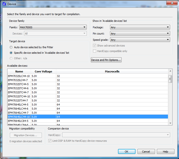
Choosing a Device
The programmable device which we'll use for our design can be chosen now.
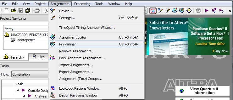
Select Assignments | Device from the pull-down menu.
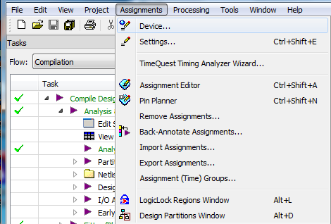
Select MAX7000S from the "Family" pull-down list.
Select the "Specific device selected" and then choose
EPM7064SLC44-10,
which is the device we are using in our lab. Select "OK."
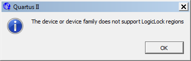
If you get a message like this, don't worry; it's fine.
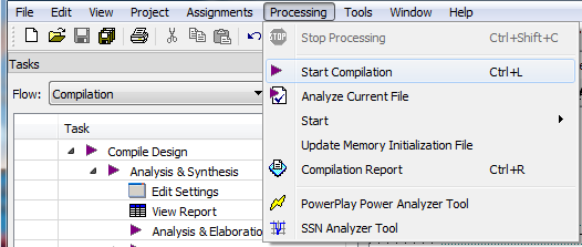
Circuit Compilation
You will need to compile
your design to ensure you do not have any errors in your circuit (e.g. you do
not have any open connections, etc.)
Click on Processing | Start Compilation to
start compilation.
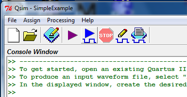
Circuit Simulation (using QSim)
If you're using a version of Quartus II lower than
13.0, use the
instructions for earlier versions.
Simulation using QSim for version 13.0
Note: In version 13.0 of Quartus II, QSim can be
opened
directly from within Quartus
II, however it only works with Cyclone devices. If you've
already chosen a non-Cyclone device, switch to a Cyclone device to do
the
simulation. Once you know your logic is correct, you can switch back to
your original device.
-
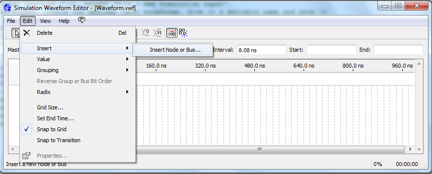
To open QSim, File | New | New University Waveform File.
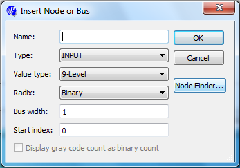
- Select Edit | Insert | Insert Node or Bus.
- Select Node Finder.
-
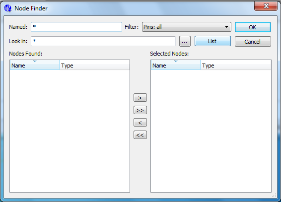
Select List.
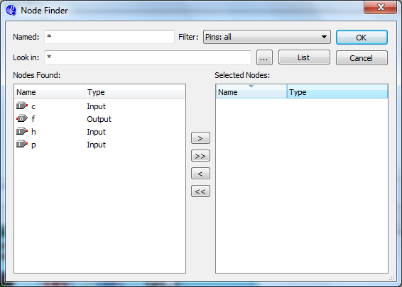
- Select the double right arrow to choose all.

-
Select OK.
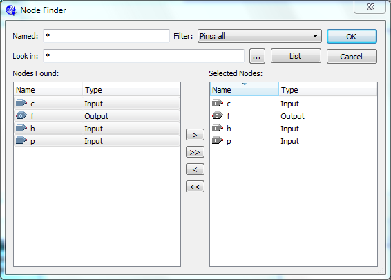
- Select OK.
-
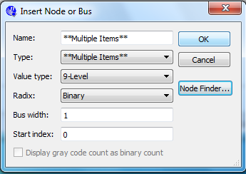
If you have multiple inputs, you can select a bunch and group them
with one counter.
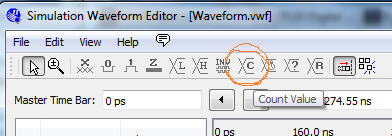
- Select your input(s), and pick Overwrite Count Value.
Select OK.
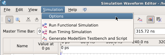
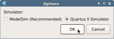
- In the Main window, select Simulation | Options
and
then select Quartus II Simulator.
Select OK.
Note: If you haven't chosen a Cyclone device, the
Quartus II Simulator option will be greyed out.
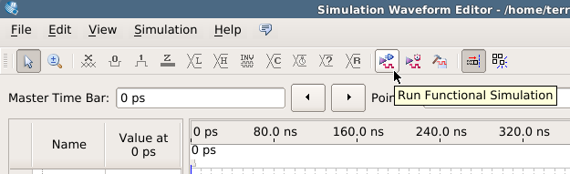
- In the Main window, select Simulation
and
then select Run Functional Simulation.
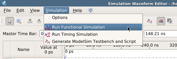
( Alternatively, you can you the button on the tool bar.)
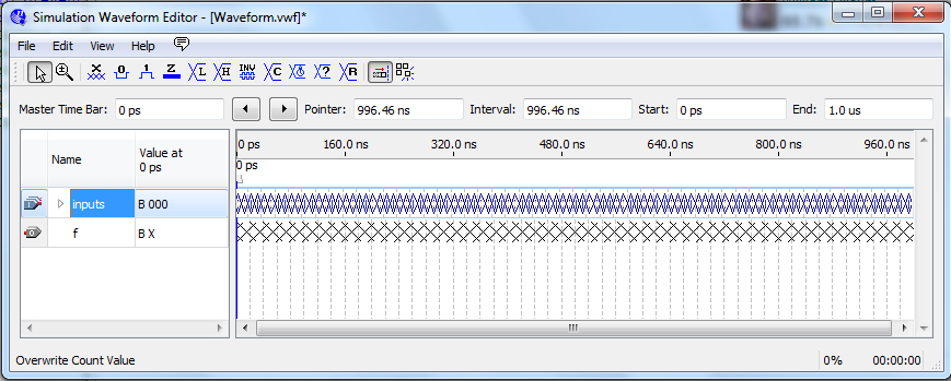
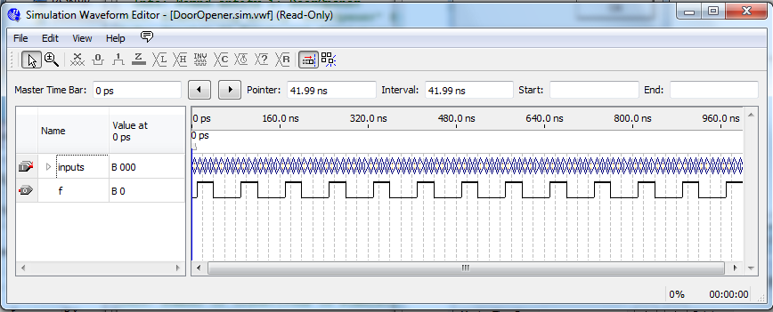
- Now you should see your simulation output with the outputs
defined. Note: The file will indicate "read-only" meaning you
can't edit it.
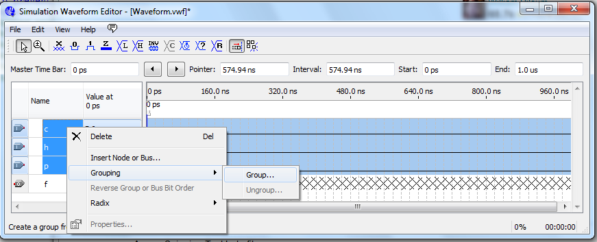
You can expand the grouping:
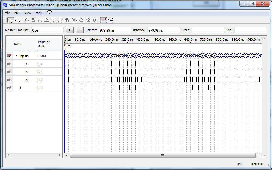
- You can navigate around the timeline, zoom in and out, etc.
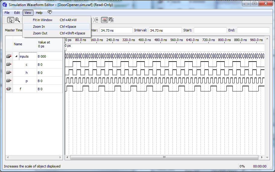
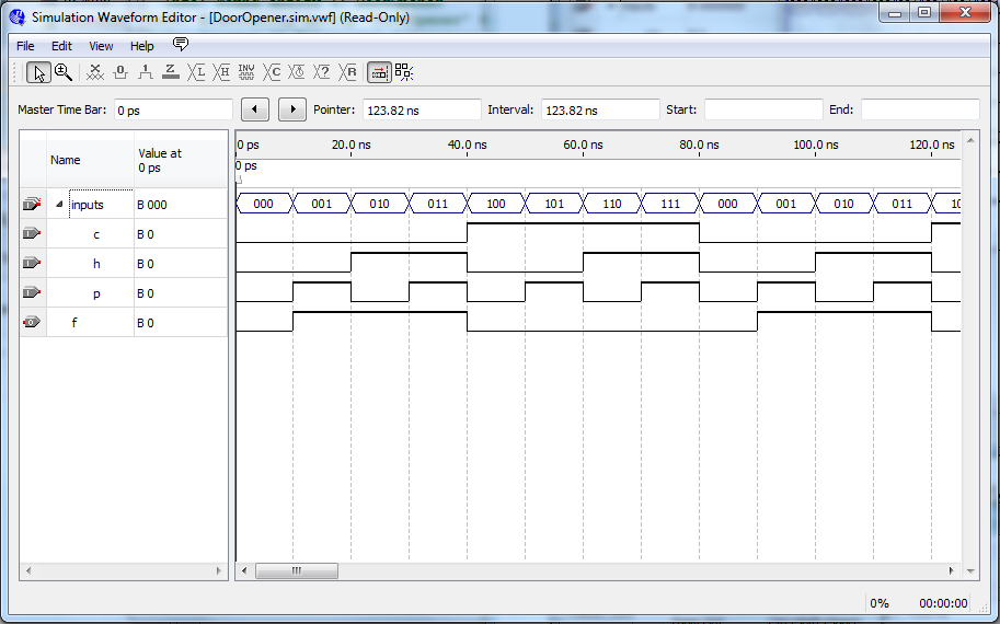
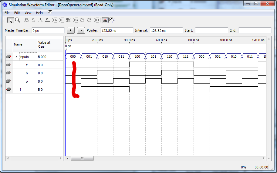
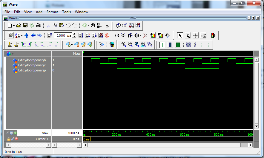
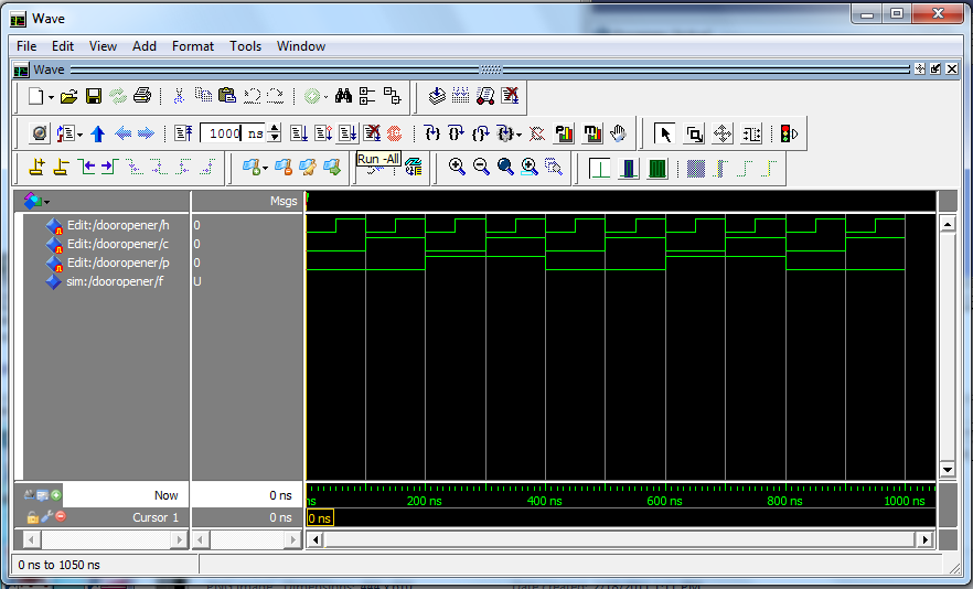
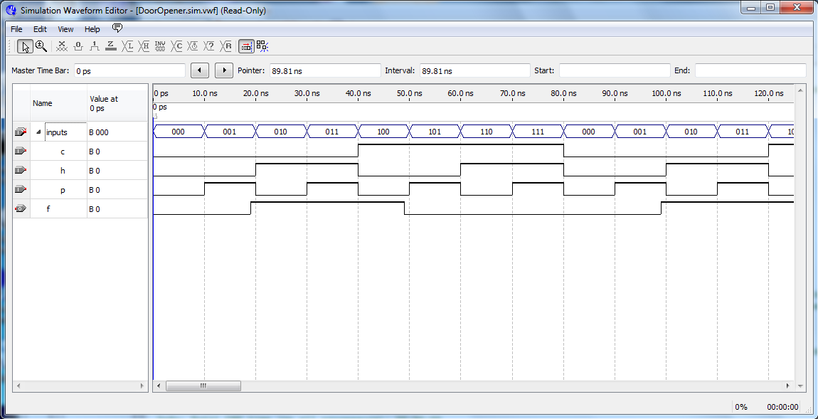
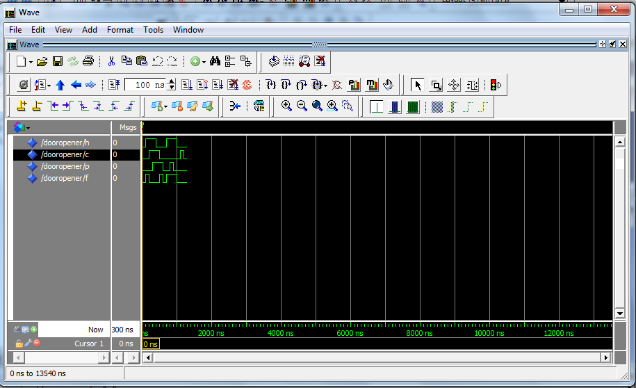
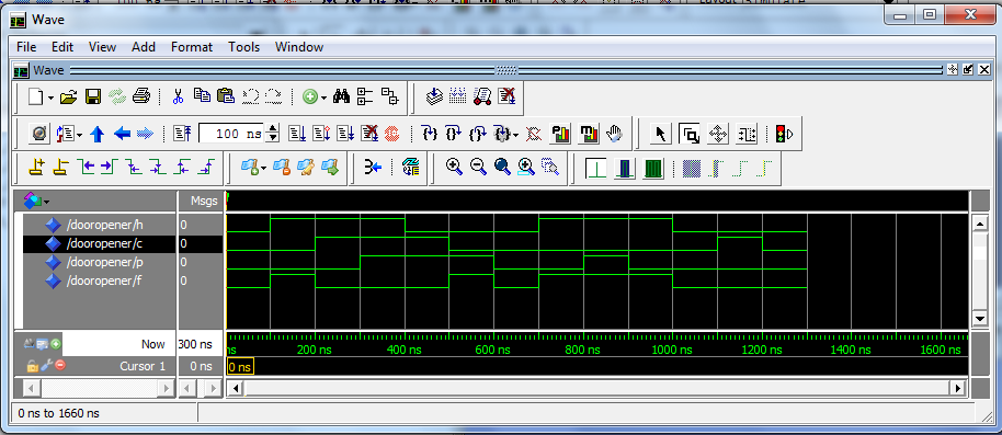
This part of the output shows that when the inputs are all zero,
the output is also zero.
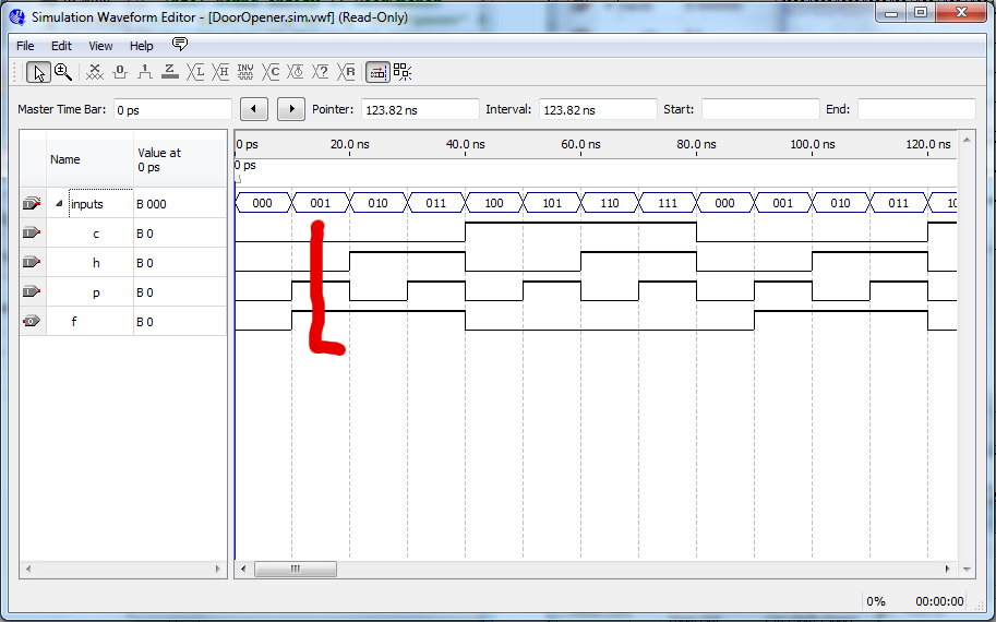
This part of the output shows that when
c and
h
are low,
and
p is high,
the output is high.
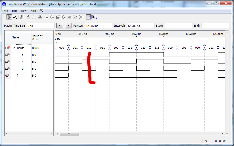
This part of the output shows that when
c and
p
are low,
and
h is high,
the output is also high.
You can repeat this process to check all of the eight
possible input combinations.
- Now if you want, you can go back to the simulation settings
and choose Timing instead of Functional to see the
effects of
propagation delay.
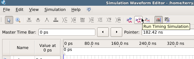
In the Main window, select Simulation
and
then select Run Timing Simulation.
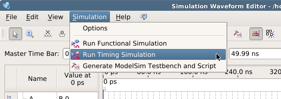
( Alternatively, you can you the button on the tool bar.)
To program a device, go to
Programming CPLDs
Simulation using QSim for versions 11 and 12
Note: QSim can't be opened automatically from within Quartus
II. You can invoke it by typing
quartus_sh --qsim
at a command prompt. (Run this in the directory where you find the
Quartus II executable file.)
- Open the Altera U.P. (University Program) Simulator, also called
QSim.
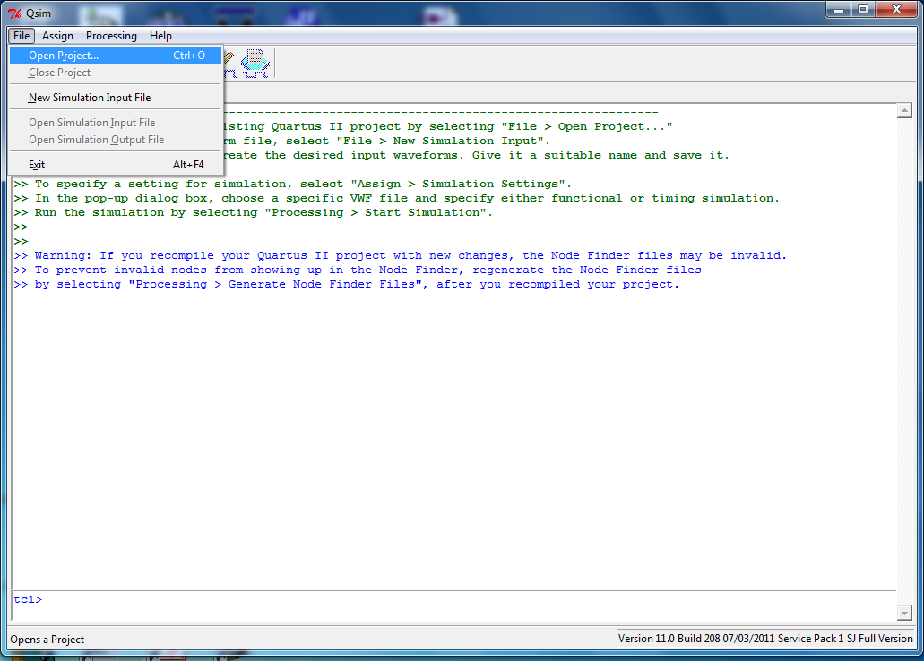
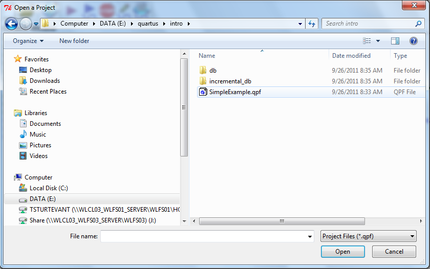
- Select File | Open Project and choose your project file
from
your project directory.
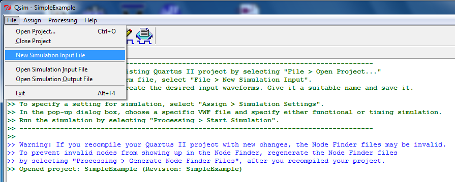
- Select File | New Simulation Input File.
- Select Edit | Insert | Insert Node or Bus.
- Select Node Finder.
-
Select List.
- Select the double right arrow to choose all.
-
Select OK.
- Select OK.
-
If you have multiple inputs, you can select a bunch and group them
with one counter.
- Select your input(s), and pick Overwrite Count Value.
You can change the rate at which a counter counts using the dialog.
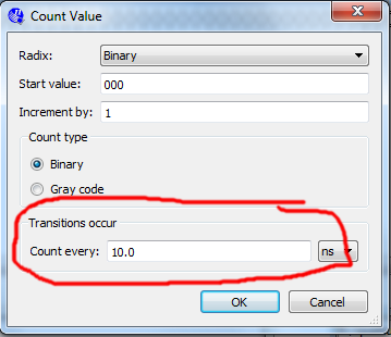
Select OK.
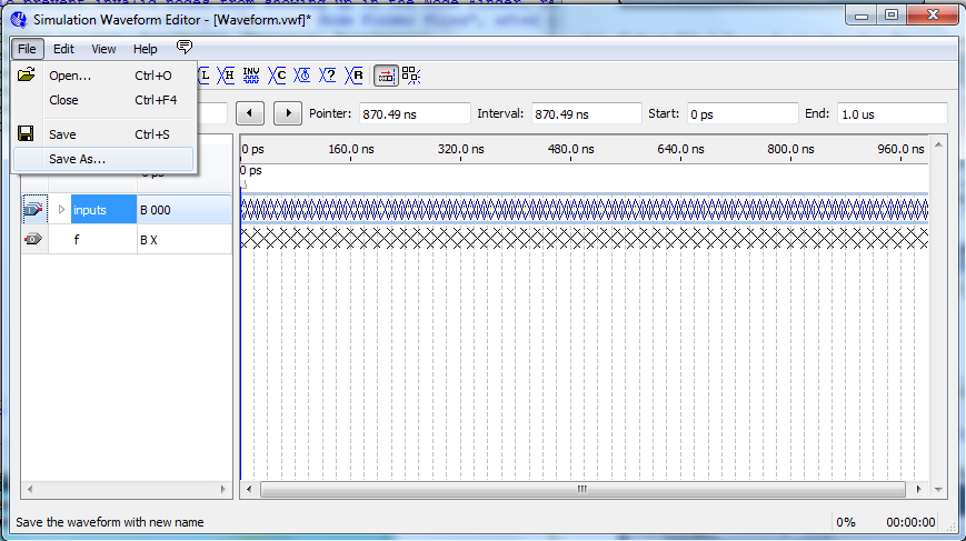
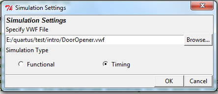
- Select File | Save As to give this file a name in your
project directory. It will have a VWF extension for Vector Waveform File.
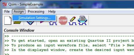
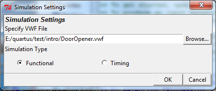
- In the Main window, select Assign | Simulation Settings
and
then select the file. Select Functional Simulation.
Select OK.
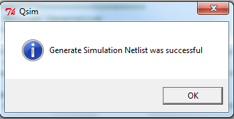
- Click the Start Simulator button.
- You should get a message saying "Generate Simulation Netlist
was succesful". Click OK.
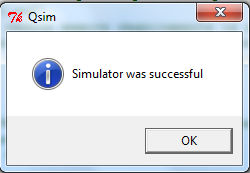
- You should get a message saying "Simulator was succesful".
Click OK.
- You should get a message from Quartus saying "This file is
read-only and cannot be edited". Click OK.
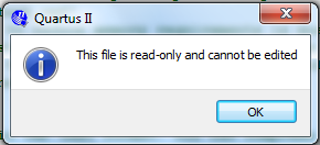
- Now you should see your simulation output with the outputs
defined.
You can expand the grouping:
- You can navigate around the timeline, zoom in and out, etc.
This part of the output shows that when the inputs are all zero,
the output is also zero.
This part of the output shows that when
c and
h
are low,
and
p is high,
the output is high.
This part of the output shows that when
c and
p
are low,
and
h is high,
the output is also high.
You can repeat this process to check all of the eight
possible input combinations.
- Now if you want, you can go back to the simulation settings
and choose Timing instead of Functional to see the
effects of
propagation delay.
Go to
Programming CPLDs
Circuit Simulation (using ModelSim)
Before simulating, some preparation is required.
Configure NativeLink settings:
- NOTE: This is DONE ONCE PER PROJECT and the information is
stored
with the project information.
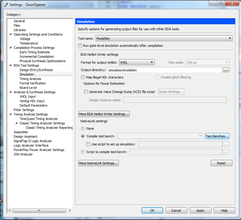
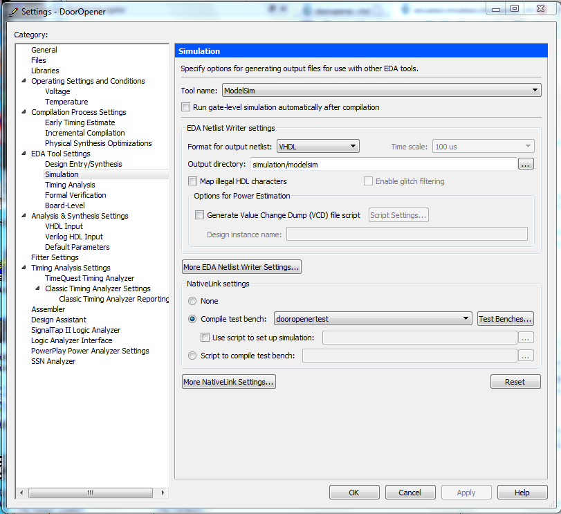
- Select Assignments | Settings.
The Settings dialog box appears.
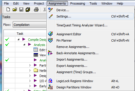
- In the Category list, select EDA Tool Settings | Simulation .
The
Simulation page appears.
- In the Tool name list, select ModelSim. [Do not turn on
Run
gate-level simulation automatically after compilation.]
- Format for output netlist should default to VHDL and the output
directory to simulation/modelsim. [Select/enter if necessary.]
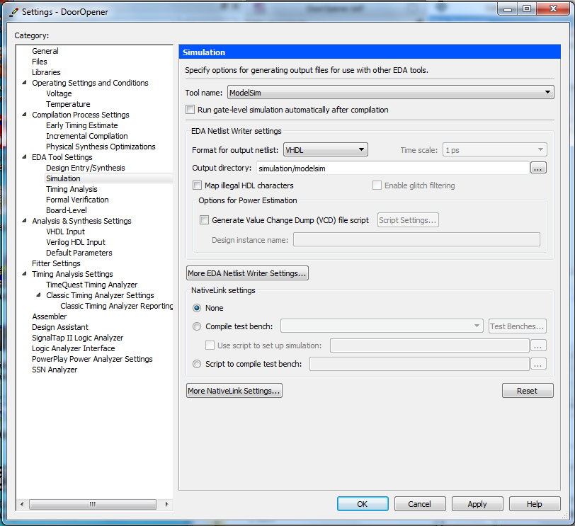
- Select More EDA Netlist Writer Settings and change the
following
options:
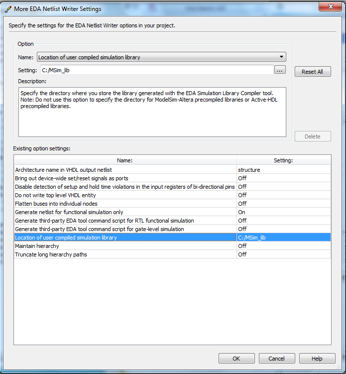
- Turn ON Generate netlist for functional simulation
only.
- Enter the Location of user compiled simulation library,
e.g.
C:/MSim_lib [if necessary].
- Select OK.
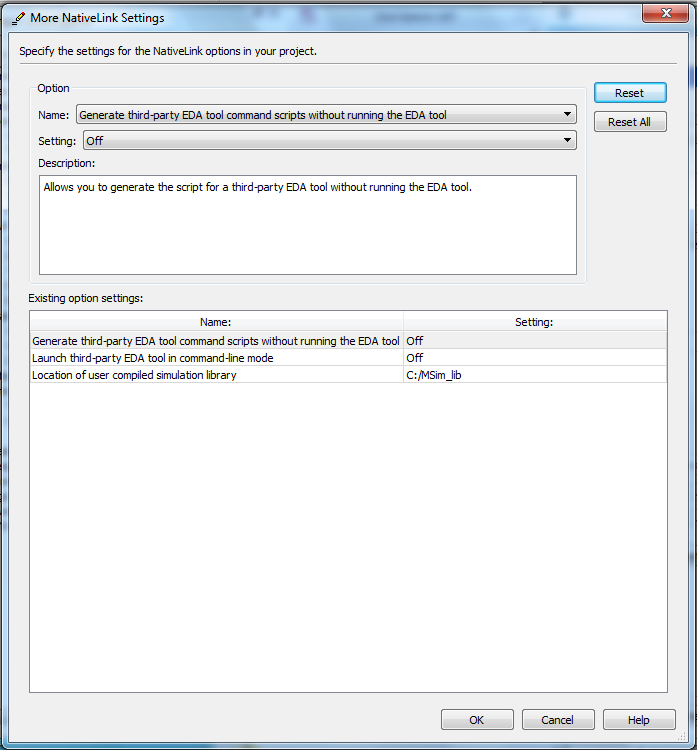
- Select More NativeLink Settings and change the following
option:
- Enter the Location of user compiled simulation library,
e.g.
C:/MSim_lib [if necessary].
- Select OK
Convert the schematic diagram into VHDL code for
simulation.
- ModelSim requires that the system be specified in an HDL
(Hardware Definition Language); we will
be using VHDL
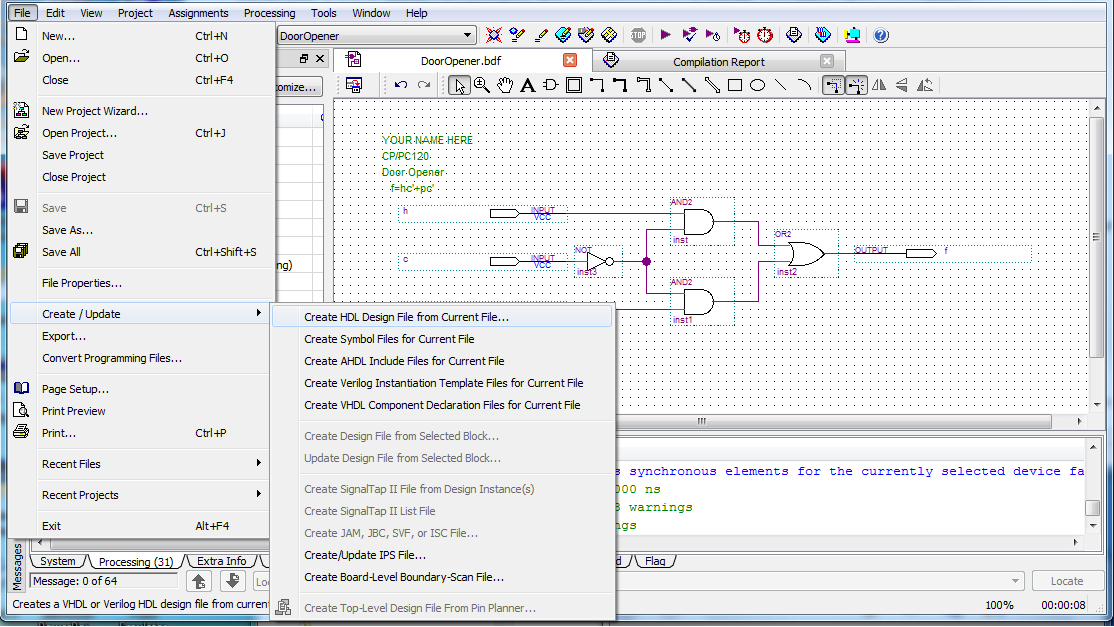
- Have the schematic open and then select
File | Create/Update |
Create HDL Design File from Current File.
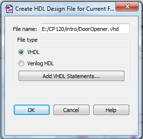
- In the pop-up window, select file type as VHDL
and the file
name will show the name and path of the file.
The VHDL file and the BDF file have the same name but
different extensions (for example, if your BDF file
is example.bdf, the VHDL file created is example.vhd).
Add the VHDL file to the project and
compile for simulation.
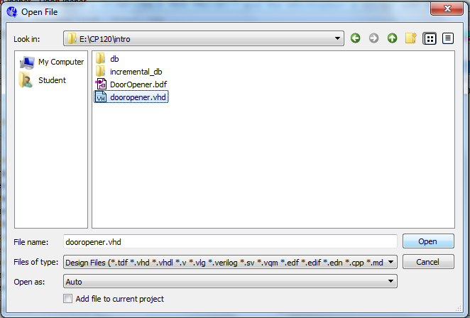
- Open the VHDL file using File | Open.
Then add it to the project
using Project | Add Current File to Project.
+ Note: The VHDL file has three parts:
- the library definitions including work where your project will
be stored,
- the entity definition which is a wrapper that defines the
inputs and outputs to the design component, and
- the architecture which defines what your component does.
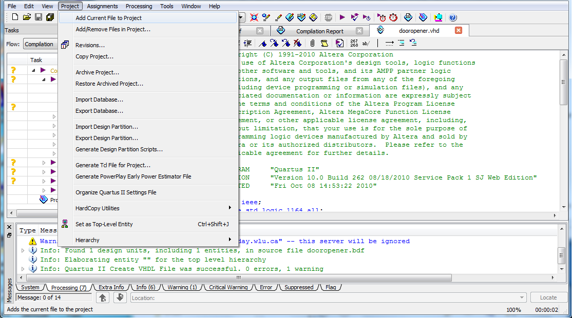
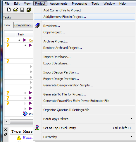
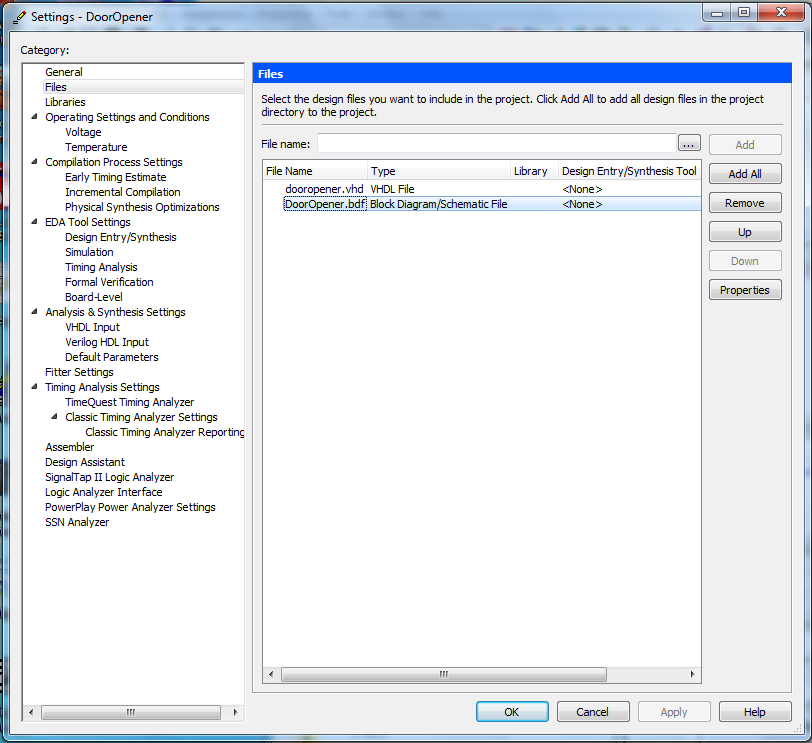
- Remove the BDF file from the project (system can't handle two source
files for the same circuit) by selecting Project | Add/Remove Files
in Project
and then selecting the BDF file and Remove.
Note that this does not delete the file (and we do not want to
delete the file).
(You don't even need to close it.)
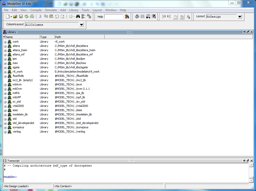
Library Compilation
It may be necessary to compile the libraries for your device family
before you simulate.
If you are using Modelsim-Altera, you will not need to do this.
All of the libraries are precompiled. If you are using Modelsim, you
may need to do this.
Click on Tools | Launch EDA Simulation Library Compiler.
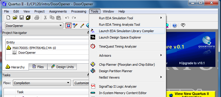
The MAX7000S family should already be selected, so
click
Start Compilation.
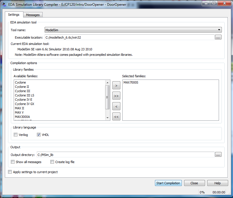
Don't worry if you get any error messages.
Methods for Simulation (using ModelSim)
There are three different methods for simulation. The simplest is using
forced inputs. It is easy to use with very simple circuits, but is cumbersome with more complicated ones.
The next method uses waveforms, which is slightly more complex but well suited to combinational
circuits where all that is needed is to go through all possible input combinations.
The last method uses testbenches, which is the most complex but the most powerful.
For sequential circuits where specific sequences of inputs must be tested, it is essential.
Simulation using Testbenches
Create a testbench to automate your simulation.
- You can get Quartus to produce a shell testbench
file by selecting
Processing | Start | Start
Test Bench Template Writer.
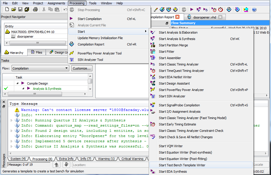
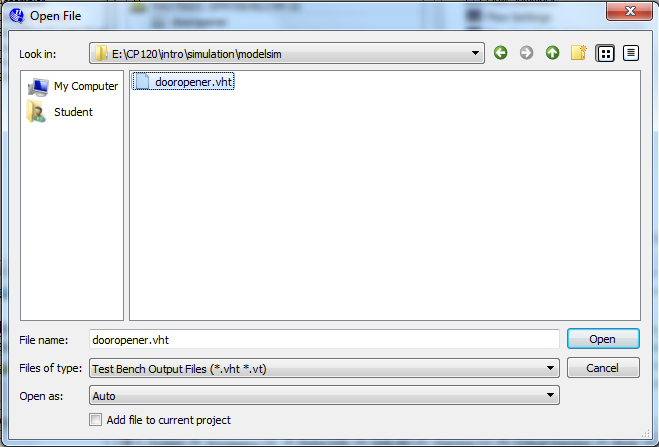
There will now be a file in your
simulation\modelsim directory.
Open it.
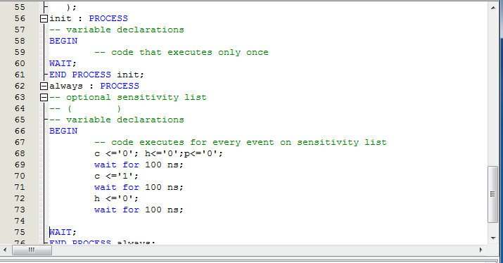
- The section near the bottom of the file is where
you put statements for your simulation.

Insert instructions for how you want the inputs to change through the
simulation.
Here's an example of the beginning for a very simple simulation:
- After making the changes, you need to change the settings
to include your testbench.
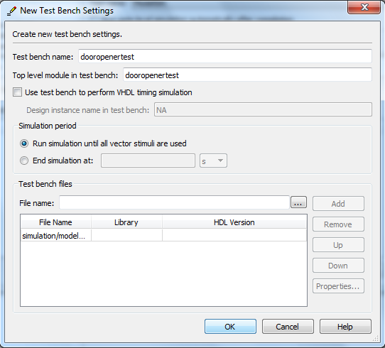
Choose a New testbench.
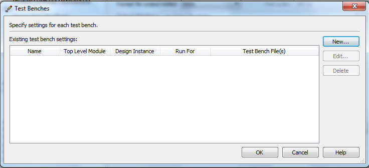
Give the test bench a name. It doesn't have to be the same as the
file name.
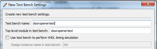
Now add the testbench file.
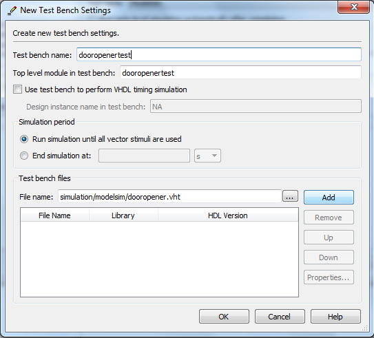
Select OK to close the New Test Bench Settings window..
Select OK to close the Test Benches window..
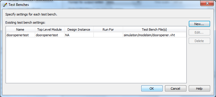
Select OK to close the Settings window..
Add the testbench VHDL file to the project and
compile for simulation.
- If it's not open, open the testbench VHDL file
using File |
Open.
Then add it to the project
using Project | Add Current File to Project.

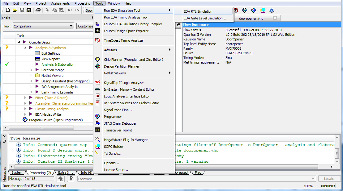
Launch the ModelSim simulator.
- Compile the circuit for a functional simulation by
selecting
Processing | Start | Start Analysis &
Elaboration.
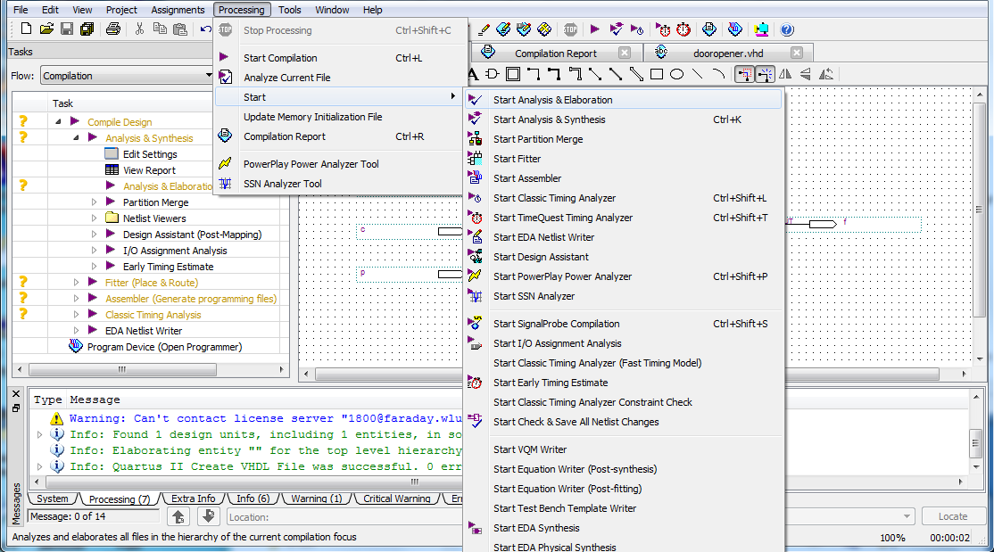
- Select Tools | Run EDA Simulation Tool |
EDA RTL Simulation.
ModelSim will display splash screen. ModelSim will
load libraries and compile the project.
The transcript pane at the bottom of the screen
indicates the scripts
that have been run (or are running).
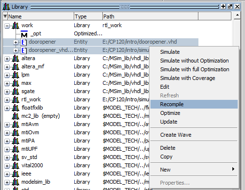
- Now your work library will
contain two VHDL files; your circuit and your
testbench. Select both,
and right click to compile both.
- Select Simulate | Start Simulation to put
ModelSim in simulator mode.
The Start Simulation Window opens.
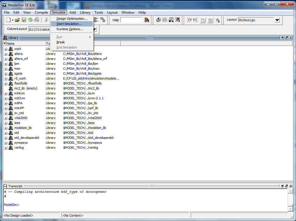
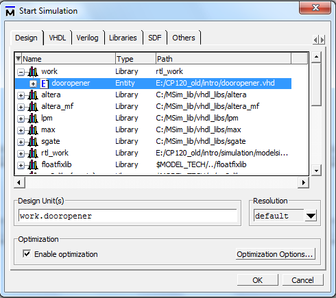
- The Start Simulation window contains many tabs.
The Design tab lists the designs available for
simulation; most are system libraries.
At the top of list will be work (default name for the
library containing your program),
expand work by selecting the '+'.
All components in your design will be listed, select
the component that is the testbench.
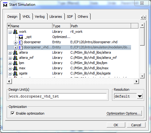
Select OK.
This will bring up other panes.
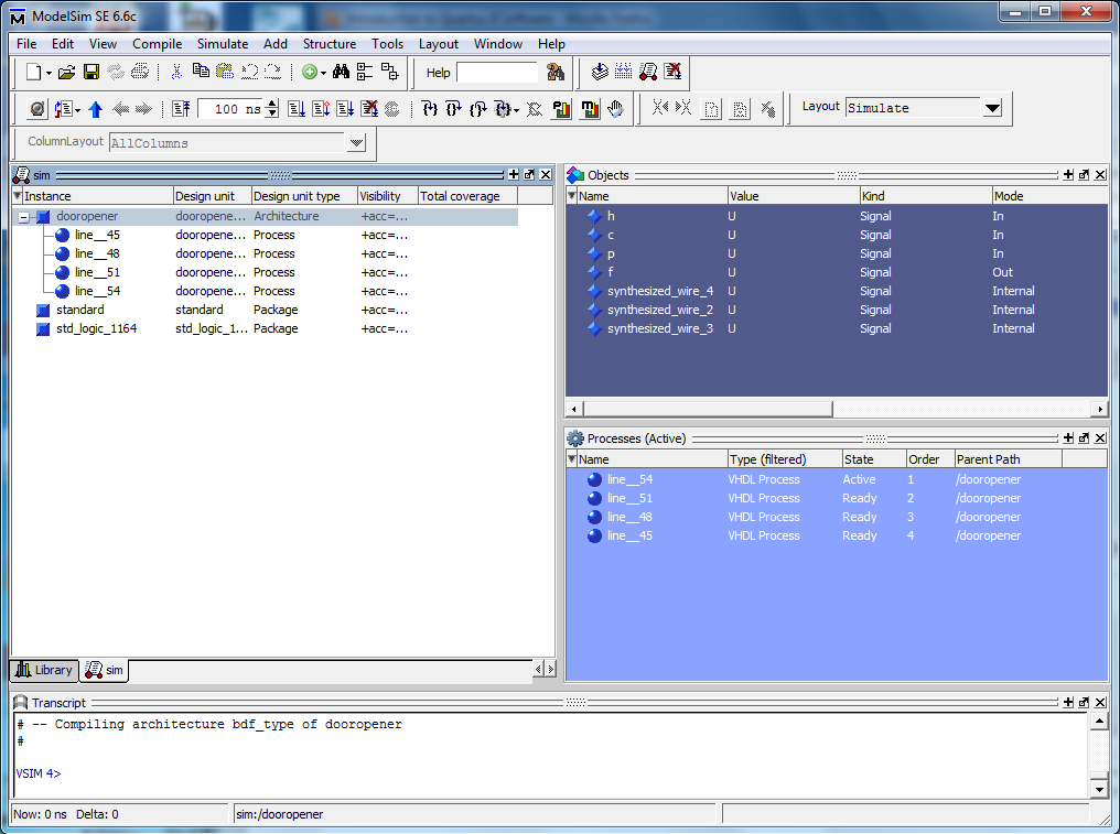
- Then the left hand side of the screen should now contain a
sim tab that displays the design units in your circuit
and the supporting libraries.
When a design unit is selected in the sim tab,
the corresponding signals are shown in the objects
window on the
right hand side of the screen.
Signals that are preceded with a plus (+) sign indicate
a bus (a group of wires with common function).
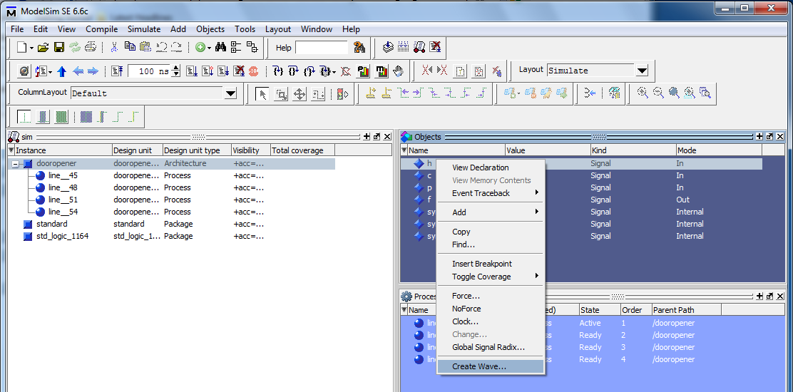
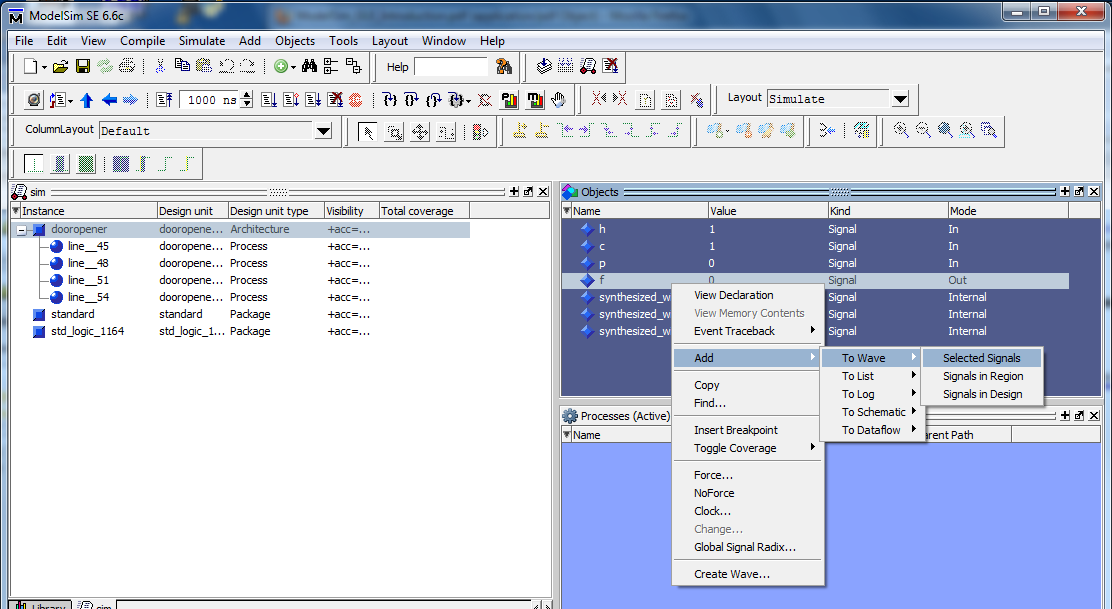
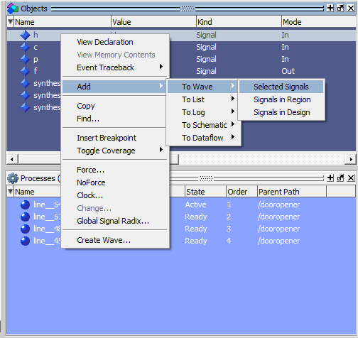
Open waveform window and add signals to be simulated.
- For each signal that you want to add to the simulation,
right click on the signal name in the Objects window
and
select Add | To Wave | Selected Signal.
Typically, you would want to add all inputs and
outputs.
A waveform window will appear in the work area.
- Alternatively, you can add a range of signals at
once by
selecting the 1st signal and then, while holding down
the shift key,
select the last signal in the range.
Then right click in the selected signal region and
select Add | To Wave | Selected Signals.
A waveform window will appear in the work area.
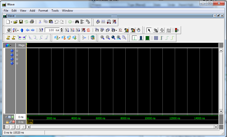
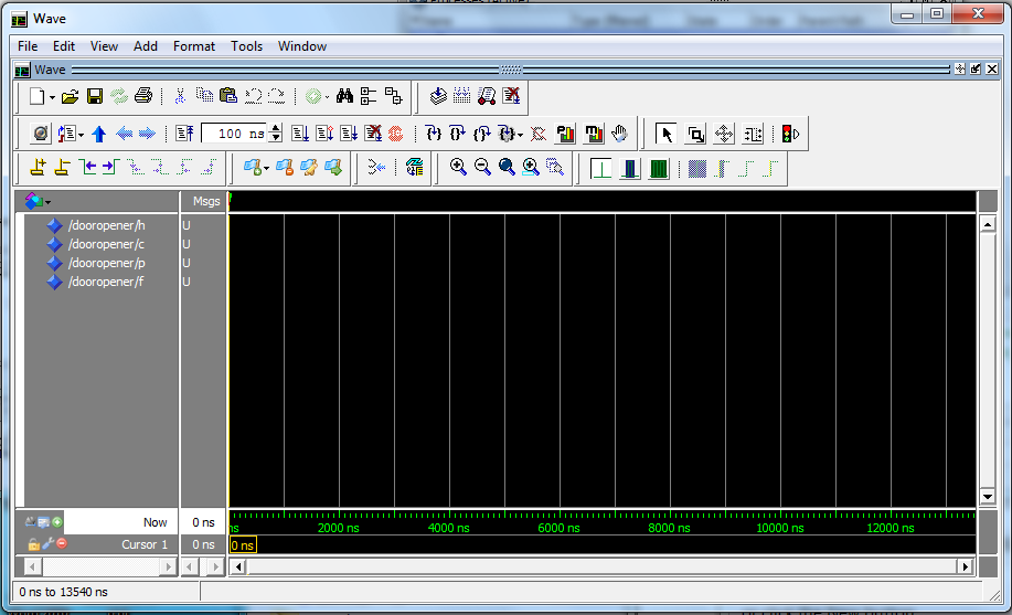
- When all signals are selected, expand the Wave
window.
- If the Wave window is not floating above the ModelSim
main screen,
use the top left icon in the wave window to undock the
window. Expand the detached window.
- In the tool icons, find the window that contains
the period of the signal,
e.g. 100ns. Immediately to the right of that window
will be the
run simulation icon (looks like a page with a blue
down arrow beside it).
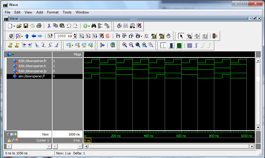
Click on it to run the simulation.
-
You should see the inputs that you entered and the
outputs from your system on the waveform.
The period of the run will correspond to the time in
the period window.
All signals should be green.
If any signals are red, then
one or more of the inputs was not specified.
Go to Examining the Output
Simulation using Forced Outputs
Launch the ModelSim simulator.
- Compile the circuit for a functional simulation by selecting
Processing | Start | Start Analysis & Elaboration.
- Select Tools | Run EDA Simulation Tool | EDA RTL Simulation.
-
ModelSim will display splash screen.
ModelSim will load libraries and compile the project.
The transcript pane at the bottom of the screen
indicates the scripts
that have been run (or are running).
- Method 1 Expand the "work" library, and start the simulation of the VHDL
file by right-clicking on it and choosing Simulate.
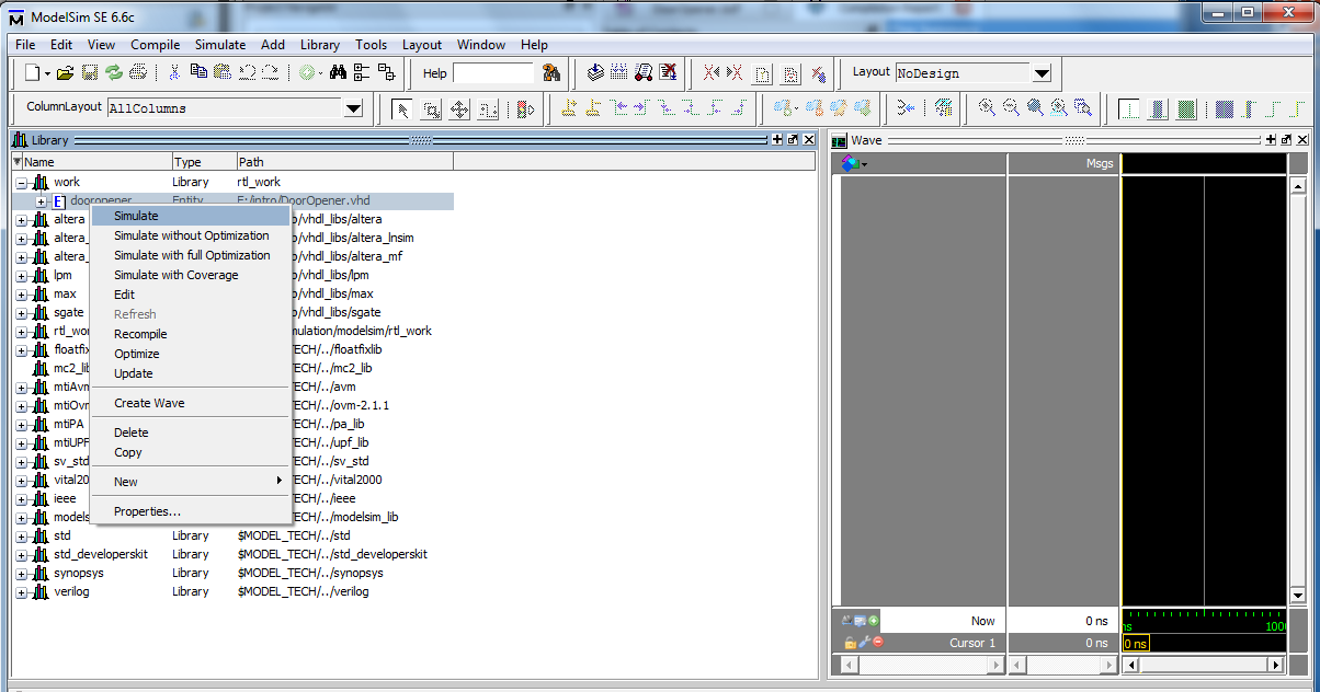
- Method 2 Select Simulate | Start Simulation to put ModelSim in
simulator mode.
The Start Simulation Window opens.
- The Start Simulation window contains many tabs.
The Design tab lists the designs available for simulation;
most are system libraries.
At the top of list will be work (default name for the
library containing your program),
expand work by selecting the '+'.
All components in your design will be listed, select the component
(or the top component in a hierarchical design).
If appropriate, turn off optimization. Select OK.
- Then the left hand side of the screen should now contain a
sim tab that displays the design units in your
circuit and the supporting libraries.
When a design unit is selected in the sim tab,
the corresponding signals are shown in the objects window on the
right hand side of the screen.
Signals that are preceded with a plus (+) sign indicate
a bus (a group of wires with common function).
Open waveform window and add signals to be simulated.
- For each signal that you want to add to the simulation,
right click on the signal name in the Objects window and
select Add | To Wave | Selected Signal.
Typically, you would want to add all inputs and outputs.
A waveform window will appear in the work area.
- Alternatively, you can add a range of signals at once by
selecting the 1st signal and then, while holding down the
shift key,
select the last signal in the range.
Then right click in the selected signal region and
select Add | To Wave | Selected Signals.
A waveform window will appear in the work area.
- When all signals are selected, expand the Wave window.
- If the Wave window is not floating above the ModelSim main screen,
use the top left icon in the wave window to undock the window.
Expand the detached window.
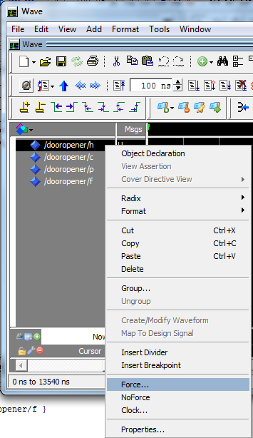
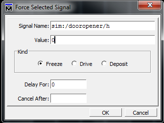
Enter signal values using force.
- To enter a signal value on a step by step basis,
select an input signal and right click on the pop-up;
select Force and for value enter either 0 or 1.
[Kind should be freeze, delay should be 0, cancel after should be
blank.]
Do this for all input signals.
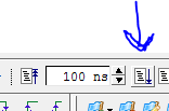
- In the tool icons, find the window that contains the period of the
signal,
e.g. 100ns. Immediately to the right of that window will be the
run simulation icon (looks like a page with a blue down arrow
beside it).
Click on it to run the simulation.
-
You should see the inputs that you entered and the
outputs from your system on the waveform.
The period of the run will correspond to the time in the period
window.
All signals should be green.
If any signals are red, then one or more of the inputs was not
specified.
- Change one of the input signals.
Select an input signal and right click on the pop-up;
select Force and for value change the 0/1 to 1/0.
Click on the icon to run the simulation again.
- Repeat until all combinations have been tested.
Go to Examining the Output
Simulation using Waveforms
Launch the ModelSim simulator.
- Compile the circuit for a functional simulation by selecting
Processing | Start | Start Analysis & Elaboration.
- Select Tools | Run EDA Simulation Tool | EDA RTL Simulation.
-
ModelSim will display splash screen.
ModelSim will load libraries and compile the project.
The transcript pane at the bottom of the screen
indicates the scripts
that have been run (or are running).
- Method 1 Expand the "work" library, and start the simulation of the VHDL
file by right-clicking on it and choosing Simulate.
- Method 2 Select Simulate | Start Simulation to put ModelSim in
simulator mode.
The Start Simulation Window opens.
- The Start Simulation window contains many tabs.
The Design tab lists the designs available for simulation;
most are system libraries.
At the top of list will be work (default name for the
library containing your program),
expand work by selecting the '+'.
All components in your design will be listed, select the component
(or the top component in a hierarchical design).
If appropriate, turn off optimization. Select OK.
- Then the left hand side of the screen should now contain a
sim tab that displays the design units in your
circuit and the supporting libraries.
When a design unit is selected in the sim tab,
the corresponding signals are shown in the objects window on the
right hand side of the screen.
Signals that are preceded with a plus (+) sign indicate
a bus (a group of wires with common function).
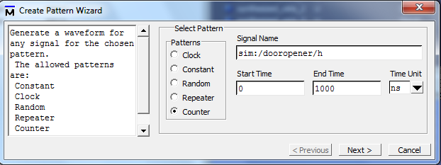
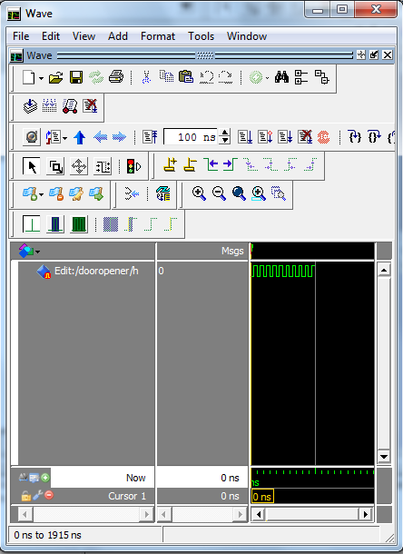
Create signals with the Waveform Editor.
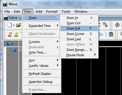
Adjusting the output display
- The output can be zoomed.
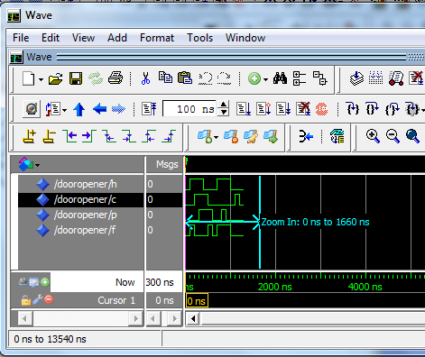
To zoom back out to see the original, you can go to
View | Zoom | Zoom Full.
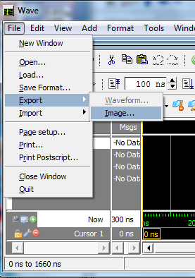
- The waveform can be exported to an image file.
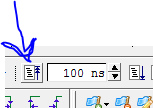
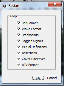
- Immediately to the left of the signal period window is the
restart simulation icon. Selecting restart will erase all signal values
entered.
Background:
Programmable Logic
Device,
or PLD,
is a
general name
for a
digital integrated circuit capable of being programmed to provide a variety of
different functions.(The "C" in CPLD stands for "complex".)
Why use a PLD?
A PLD is good for prototyping
designs. Only a single chip is required to implement a complete logic
design. It allows
us to
simplify designs and reduce development times. Changes in the design can
be easily implemented by reprogramming the device. Simple PLDs (such as the
one we
use in our lab) can realize from 2 to 10 functions of 4 to 16 variables on a
single integrated circuit
[click image to get a larger image]
Preparing the Circuit for a CPLD
If you already have a compiled design open, you can skip to
assigning pins.
Open your project
Use File | Open Project
You'll be using the door opener from before.
Select your Device
Select Assignments | Device from the pull-down
menu.
Select MAX7000S from the "Family" pull-down list.
From the "Available devices" choose EPM7064SLC44-10,
which is
the device we are using in our lab. Select "OK."
Compile
You will need to compile
your design.
Click on Processing | Start Compilation to start
compilation.
Assigning
Pins:
Select Assignments | Pin Planner from the pull-down
menu.
You'll see a schematic of your device which shows the satus of various
pins, with a list of your inputs and outputs below.
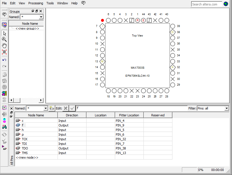
You will notice that the pins around the edges of the chip have
different symbols. The plain round circles with nothing written inside of
them are used for input and output.
Assign all of your pins to fit in one "bank" of CPLD
connections, so only one jumper cable is required.
Banks are:
For example, here is bank one.
[click image to get a larger image]
Here is bank two.
[click image to get a larger image]
Select each input and output from the bottom of the screen and
drag it on top of the pin you would like to use - make sure you click on
the name. (ie. if you want h to be pin 4, click h on the bottom of the
screen and drag it on top of the circle under the label 4).
Remember, use ONLY the plain round circles!!
You only need to assign your inputs and
outputs;
you will probably see some other signals listed that you didn't specify.
Leave them as they are.
When you are finished you can close the window.
Recompile Design
You will need to compile
your design again to fit your design on the PLD board.
Click on Processing | Start Compilation to start
compilation.
Setting up
Programming Hardware in Quartus II Software:
Connect your USB-Blaster cable to one of the USB ports on your
computer.
Note: Under linux, for the programmer to connect, do the following as
root once the programmer is plugged into the computer:
From your Quartus II binary directory, (i.e. where the quartus
executable is located), run
- jtagd
- jtagconfig
After this, the programmer should work.
Choose Tools | Programmer.
The Programmer window will open.
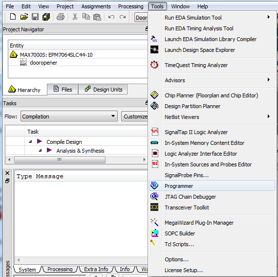
The selected programming hardware
is identified as. If it says
"USB-Blaster [USB-0] mode
JTAG" you have the correct hardware (skip to the connection step).
Click the Hardware Setup
button to open the Hardware Setup window.
Programming hardware that is
already set up appears in the Available hardware
items window.
If the USB-Blaster is not listed as the
Currently selected hardware, select it and click
the Add
Hardware.
Click Close.
At the main window, ensure it displays
USB-Blaster[USB-0] mode JTAG (see figure below)
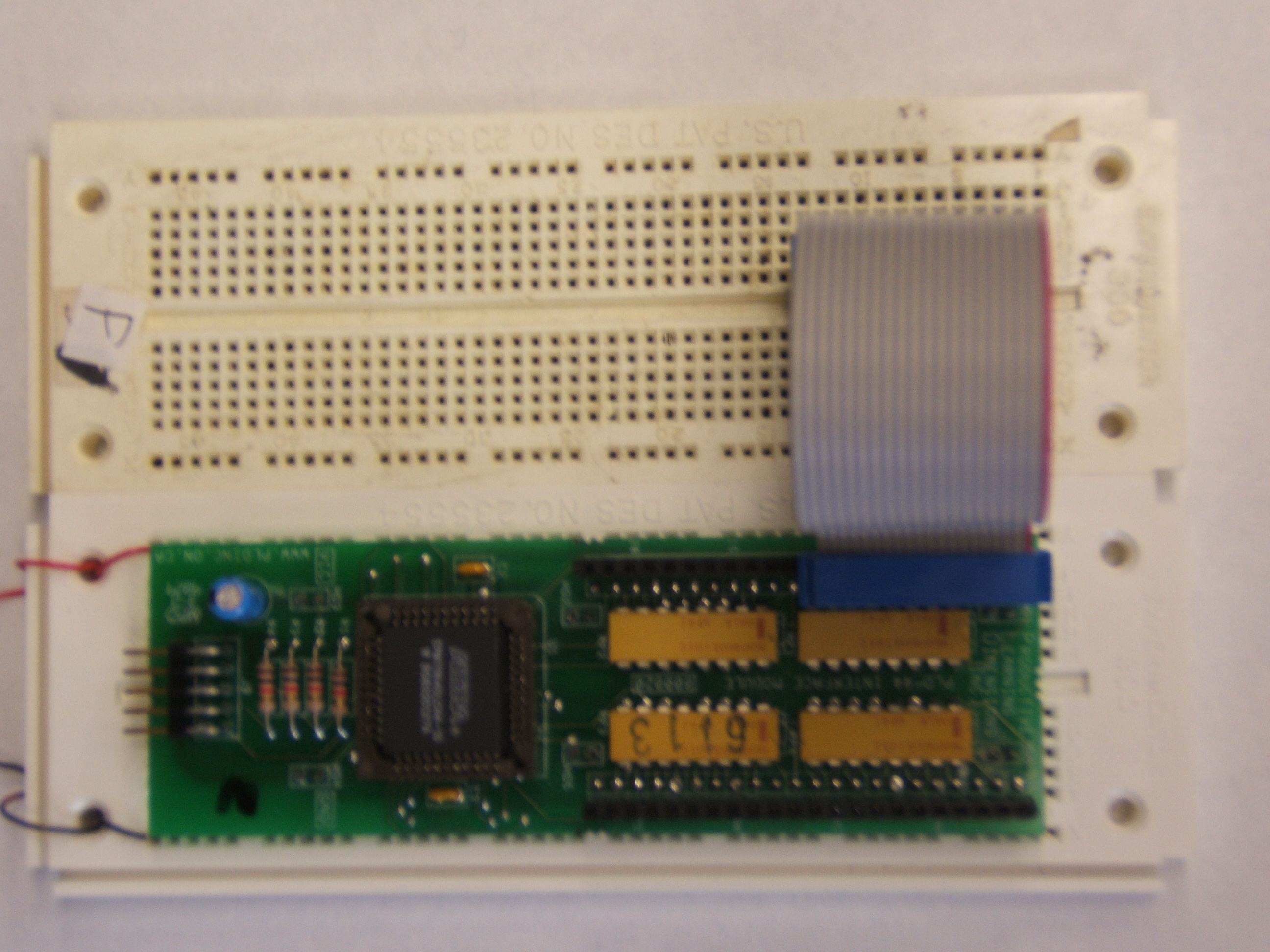
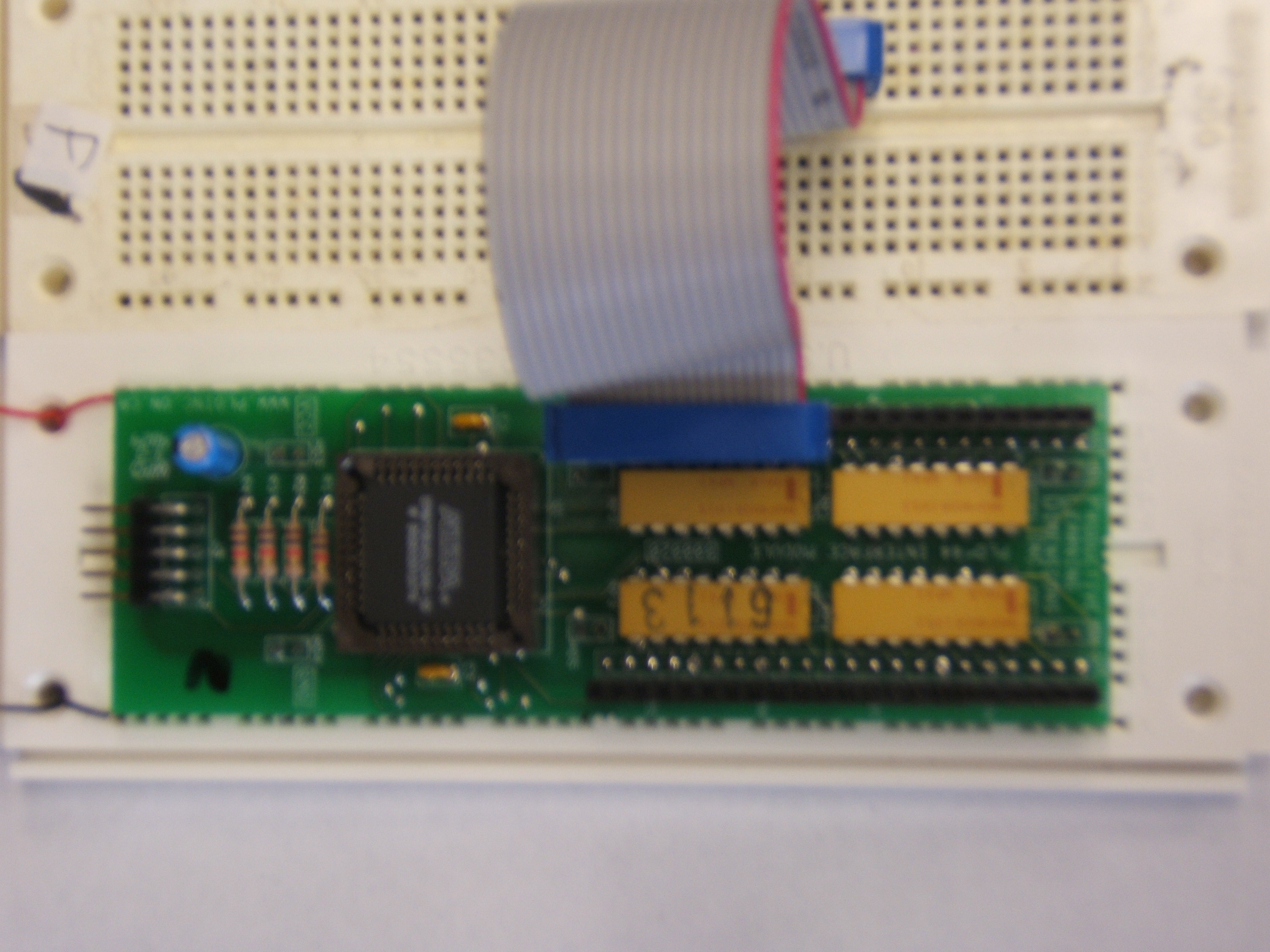
Connecting
Programming Hardware to the Device:
Connect CPLD board to USB-Blaster cable (connected to a USB port on
your PC).
The cable should be attached so that the red edge of the USB-Blaster
cable is next to the number (usually a "1" or a "2") that has been
written on the board with a marker. IF YOU'RE NOT SURE, ASK!!!
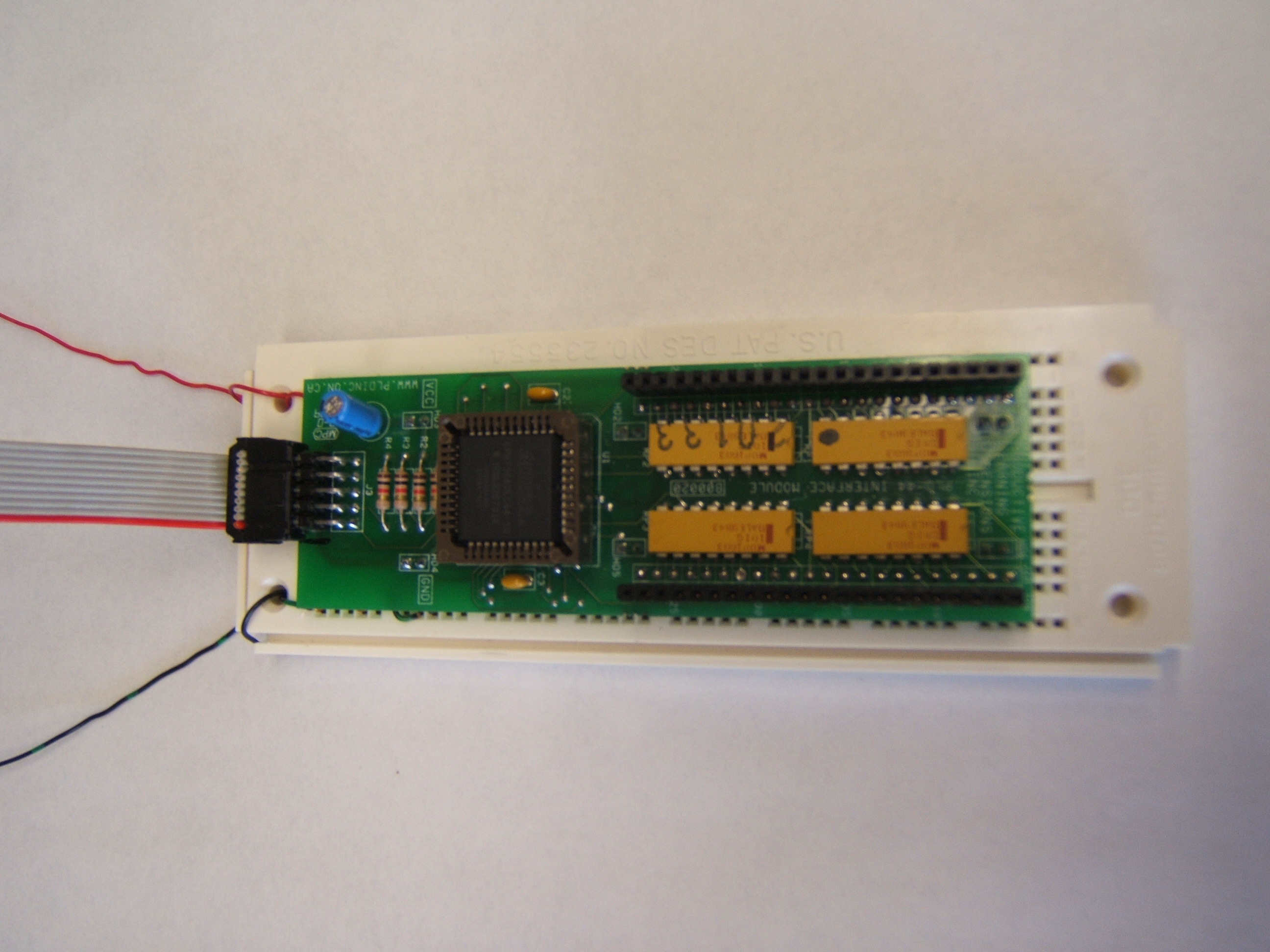
[click image to get a larger image]
Connect the ground and power (5v) to the CPLD board
and turn the power on.
Click Auto Detect, your program
should detect the CPLD.
If it doesn't, there are three possibilities:
- You haven't chosen the correct device.
- Your cables aren't connected correctly.
- Your CPLD is faulty.
| Problem |
Solution |
| Unable to scan device chain. |
This is generally a problem with power. Check:
- Is the power and ground connected properly and turned on?
- Is the red strip on the USB-Blaster cable connected to the
proper side of the board?
|
| JTAG error |
This is generally a problem with the connection. Try:
- Make sure you have the correct device selected
- ensure 7064 (not 7032)
- ensure SLC (not STC)
- Unplug the USB-Blaster cable and reconnect.
- Try a new USB-Blaster cable.
- Try a new CPLD board
|
| License error |
This is generally a problem if you haven't done anything with
the software recently.
The server times out and loses the connection to the
licencing file.
- Close Quartus and reopen.
|
Once it autodetects correctly, you can proceed.
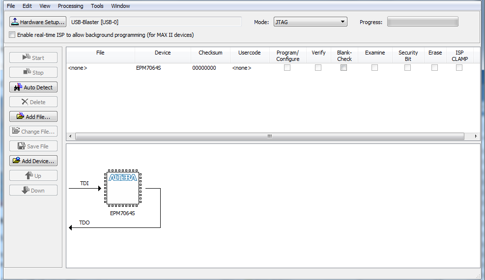
Delete the file that shows up.
Click Add File
choose 'pof' file
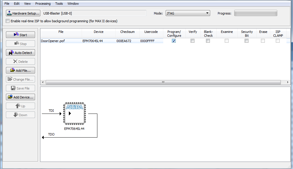
Check Program/Configure
Select Start,
you should see the progress indicator
increasing slowly (fast means problem).
Wiring the Input and Output
You can unplug the USB-Blaster cable and turn off the power while
you are wiring your circuit. You will not lose your program.
Use the debugger board to wire the input (use the
control mode) and the output (use the display mode).
(ie. c, h, p & f)
Troubleshooting
If you smell smoke turn off the power immediately and DO NOT touch
the Altera chip. It gets extremely hot if it is short circuited.
Check all your power and grounds, have someone else check your
power and grounds - something IS wrong!! Hopefully, your chip
will still work. :)
- First, double check your simulation to ensure that your
Quartus design is correct.
If it is not correct then you will not get the correct
output no matter how well
everything else is connected.
- Next, check your device, even if you think it's right... double check.
If you need to change it
make sure you recompile.
- At the top of your pin out file make sure it
reads ASSIGNED TO AN: EPM7064SLC44-10
- ensure 7064 (not 7032)
- ensure SLC (not STC)
- Check your pin assignments and make sure you have not assigned any of
your inputs or outputs
to reserved pins or specialized pins. Plain circles only
(with no writing inside).
- Make sure you have power and ground to your boards (CPLD,
debugger, breadboard).
- Make sure you have the debugger board set up for input and
output correctly.
- If some signals seem to be right and some seem to be wrong,
check your pins to make sure you
are in the correct place and use the multimeter to ensure
you have good connections.