


Implementation of a VGA Graphic Card Using a Xilinx XS95 Board
and Bonnie Hung
hung1850@mach1.wlu.ca
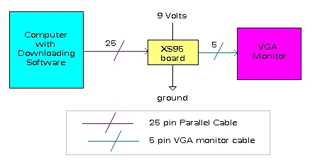
The purpose of this project was to display an image loaded into RAM, onto a VGA monitor. This was to be achieved by using an XS95-108 board. The XS95 board consists of a Xilinx XS9500 CPLD, and a 32 KB SRAM. The board also has a VGA port which allows it to connect to a VGA monitor. The port consists of 5 pins, three for colour ( red, green and blue ) and two for the syncrhonization ( one for horziontal and one for the vertical ). The board was connected to a 9 V power supply, and a 25 pin parallel port was used to download the programs into the CPLD.
Tools:

Components of interest on the Xilinx Board
Below are steps to create and download a hex file into your XS9500 board.
For the VGA monitor a frequency of 25MHz is required. This frequency is desired because it is the minimum frequency at which you will see no flicker. Flicker basically occurs when the colour guns do not paint on the screen fast enough and you can see when it is painting on the screen. What you are seeing is the refresh rate. Such things as flourcent light can also interfere with flicker occuring on the screen. A frequency of 25 MHz is required and the board is equipped with a 100 MHz oscillator. Along with the board the designers have inlcuded software. Part of this software package is a clock divisor. It is possible to divide the oscillator by entering an integer divisor. Since we required a 25 MHz clock we entered a divisor of 4. Once the clock is set, it is not necessary to reset it every time you download a new program or unplug the power source.
Now that your clock is set, you are ready to synthesize, implement, and program the clock synchronization code for VGA monitor. The tester code can be found at the XS95 Displaying a VGA Signal Manual. First, open project manager (on your desktop) and open a new project. You are now in the Design Flow pane. Click on the design entry icon to write or open your VHDL code. To check for errors, go to Synthesis and click on the "Check syntax" menu item. If there are no errors, a "check successful" should appear. Save this file and exit from the editor.
You are now back to the Design Flow pane. You should see a check mark in the design entry
signifying that that part has successfully completed. Go to Project and click on the
"Add Source" menu item to add your file into the project. Click on the Synthesis icon.
The Synthesis/Implementation settings window will pop up. The settings used for our board were as follows :
Top Level: name of our vhdl file
Version Name: ver1
Family: XC9500
Device: 95108PC84
Speed: -20
Click Run. When the code is successfully synthesized, you should see a check mark beside the Synthesis icon on the Design Flow pane. A file with extension "ucf" is automatically created in the project directory. Add the ucf file into the project by going into Project and clicking on "Add Source". The ucf file is where the pins are assigned. For a more information on the pin layout, see the Schematic Diagram section. Save your ucf file after assigning the pins.
Next, click on the Implementation icon and it will bring you back to the Synthesis/Implementation settings window. Go to "set" under the physical implementation settings and choose custom under "use constraints files from:" to select your ucf file. Click OK and click Run to start the implementation tools. A successful implementation will result in a check mark beside the implementation icon on the Design Flow pane.
Click on the program icon to get to JTAG Programmer. Go the Output and click on "Create SVF file" menu item. The SVF file is the bitstream used to load the program into the CPLD. The SVF settings window will appear. Click on Through Test-Logic Reset instead of the Skipping Test-Logic Reset. Choose where you want to save your svf file and click Save. Go to Operations and click on the "Program" menu item. On the options window, only the "Erase before Programming should be checked off. Click ok and close the JTag programmer.
Everything in the Project Manager is completed. Now you can create the Hex file. First, create a SIMPLE bmp file. Then, go to the Image Processing Tool and download the software to convert the bmp file into a hex file. Ths software was a project created by students. Unfortunately, even though it creates a hex file, the file format does not follow the intel standard format. below is one line from the hex file, and an explanation of the format to our understanding.
Figure 2: Single Line from a HEX file
- 800480FFFFFFFFFFFFFFFFFFFFFFFFFFFFFF00D0D0D0D0D0D0D0D0D0D0D0D0D0D0D0000000008080000000FFFFFF0000D0D0D0D0
FFFFFFFFFF00FFFFFFFFFFFFD0D0D0D0D0D0D0D0D0D0D0D0D00000FFFFFFFFFFFFFFFFFFFFFFFFFFFFFFFFFFFFFFFFFFFFFFFFFFFFFFFFFFFFFFFFFFFFFFFFFFFFFFFFFFFFFFFFFFFFFFFFFFFFFFFF
the -80 part means that there is eight bits per pixel. The next four numbers 0480 are the beginning address in the RAM chip where the bits will be encoded. The rest of the line is the coding for the picture. One character represents four bits, and two characters represent one pixel. This line has a width of 128 pixels, thus there are 256 characters ( not including the beginning 6 digits ) in the line.
After you have downloaded and installed the program, open it and then open the bmp file. Then just select to save as a hex file. You do have the option of having it encode the hex file with 8 bits per pixel, 4 bits per pixel, 2 bits per pixel or 1 bit per pixel. To do this just right click on the image in the program and select the number of bits per pixel. It is recommended that you chose 8 bits or 4 bits per pixel because anything less than that will reduce the number of colours in the image too much. We chose 8 bits per pixel because it is the default format.
Now, load both the synchronizing project and the hex file into the chip by opening up GXSLOAD. Drag both the svf and hex file into the window. This may take a while depending on the size of the files. A message will pop up to notify you that the chip is programmed. If everything was correctly done, including the code, you should see a representation of the image downloaded into the RAM on the screen.
The timing simulation diagram below shows a simulation of the actual tester program that was used. It depicts only a part of the timing diagram. It would take pages to show the full time it takes to write out the signals to the entire visible and non-visible region of the screen.
The important signals to look at are vsyncb, hsyncb, oeb, and rgb.
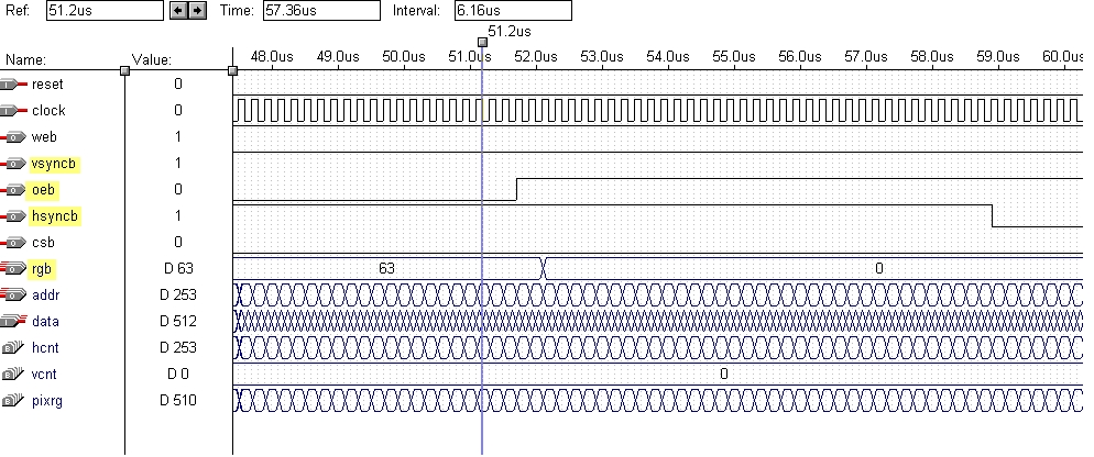
vsyncb : is high on this portion because we are writing one horizontal row of pixels. It will go low for a pulse period when we are at the bottom of the visible region of the screen.
hsyncb: at around 59 us, the hsyncb pulse goes from a high to a low. At this time we have gone beyond the visible region of the screen and finished writing the line. It is pulsing low for a time period to indicate this and to co-ordinate with the vertical timing.
oeb : this signal is the read signal from the RAM chip. While it is low, we are reading from the RAM and producing and output on the screen ( see the rgb signal ). When it goes high, we stop reading from the RAM because we are at the end of the line and do not need to read anything. (ie: there is no point in reading anything if we are not in the visible region of the screen.)
rgb : on this section , the colour being displayed on the screen is red. Further along in the timing, you would see this colour changing. You can also see, that it goes to 0 when oeb is enabled because we are in the non-visible region.
Intital Tester Code
The tester vhdl code that was first used can be found at the XS95 Displaying a VGA Signal Manual. There is also ABEL code available if you would like to program the board using ABEL. No modifications are necessary to to the vhdl code. The only modifications necessary are the pin assignments. The documentation list the pin assignments as : 002- NET CLOCK LOC=PIN9; When creating the UCF file you omit the preceeding number and dash ( ie: the "002 -" part ).
Also, the UCF file must correspond to your vhdl code not the pin table listed in the XS95 manual. If you named your clock_25MHz in the VHD file you would write NET clock_25MHz LOC=PIN9; even though in the pin table of the documentation the clock is label as clock. The pin list in the manual listed above does not do this. In their vhdl code they use hsyncb but the pin assignments are listed using the default manual names. They also list two pins that are not used in the vhdl code, namely RST and XTAL1. If you include unused pins in your UCF file, or if you don't use corresponding names you will get an error when you try to implement the program. Here is the code typed out in a vhdl file. vgacore.vhd All the explanation for the code can be found at the tester link above and we feel no more additional elaboration can be made on it.
NOTE: all the follow code was used by modifying the tester code. This is because the tester code included the basic syncrhonization timing that is necessary when deisplaying an image on a monitor.
Code without using the SRAM
First the tester code was manipluated without using the data in the RAM to display a pattern on the screen. This code can be found here pattern.vhd.The follow section of codes are the two most important parts in creating the pattern so we will look at them in further detail.
Part 1
-- this creates an address to reference to, but we are using that
-- address number to create a pattern ignoring what ever data might
-- be contained in the address
H: addr <= vcnt(1 downto 0) & hcnt(3 downto 0);
Part 1 shows how the program decides to write to the screen. The vertical count and the horizontal count were used to reference an address line and then combined them into a temporary register. The pattern is created because only the lower four bits of the horizontal count are referenced, and only the lower two bits of the vertical count are referenced. Thus , every time these repeat, the pattern will repeat.
Part 2
-- map the pixel to a color if the video is not blanked
if pblank='0' then
case pixrg(5 downto 0) is
when "010001" => rgb <= "110000"; -- red
when "010010" => rgb <= "110000";
when "010110" => rgb <= "110000";
when "010111" => rgb <= "110000";
when "100001" => rgb <= "010001"; -- dark purple
when "100010" => rgb <= "010001";
when "100110" => rgb <= "010001";
when "100111" => rgb <= "010001";
when "110011" => rgb <= "000011"; -- blue
when "110100" => rgb <= "000011";
when "110101" => rgb <= "000011";
when "000011" => rgb <= "001010"; -- teal
when "000100" => rgb <= "001010";
when "000101" => rgb <= "001010";
when others => rgb <= "111111"; -- white
end case;
Part 2 shows the colour assignments according to what is sitting the in temporary register. Every time one of these specific combinations occur, the pixel is painted its assigned colour. the RGB colour consists of 6 bits, the two most significant bits correspond to red, the two middle bit correspond to green and the two lower bits correspond to red. This code was designed this way for simplicity and that the board only supports two bits per colour. The RGB colour vector is represented this way in all the codes that were used.
The image we saw on the screen looked like this :
Colour VHDL using the SRAM
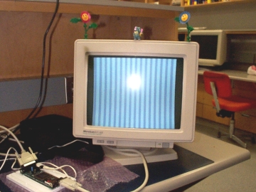
It was discovered that images could be loaded into the RAM using a HEX file. How to do this is outlined in the block diagram section. The HEX file ( colour.hex ) was created using 8 bits per pixel and we encoded the file to have 64 different code combinations. 64 code combinations were chosen because that is the maximum number of colours available when there is three colours, namely red, green and blue, with 2 bits per avaiable per colour. The original tester program was also modified. The new code can be found here colour.vhd. It was noticed that the when using the horizontal count and vertical count to reference an address the image size had to correspond with the address count. If the lower 7 bits of the horizontal count are used, this gives a total of 27= 128 bits. Therefore the image being used should have a width of 128 pixels. Since we are using lower 7 bits of the horizontal count , and there are 15 address lines, it is possible to only use 8 bits from the vertical count. This combination makes the image repeat itself 4 times on the monitor because the total width of the visible screen is 256 ( 2 times 128 ) and the total length of the visible screen is 480 ( which is approximately 2 times 256, the maximum number we are referencing with the vertical count ). Since our HEX file has 64 combinations, 64 differenc colours were used, with one combination corresponding to one possible colour. The data loaded from each address contained one pixel, which was then assigned a colour to it depending on the coding we chose. The colours were displayed chromatically by using "000000" ( this equal black ) as the first colour, and "FFFFFF" as the last colour (white).
The image we saw on the screen looked like this :

Snoopy VHDL using the RAM
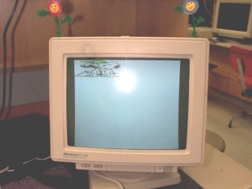
The following VHDL code is very similar to the colour vhdl code. We loaded the following snoopy picture ( see figure 3 ) into the RAM and altered the HEX file by colouring in different sections. We also only diplayed one image of the snoopy picture onto the screen by limiting when we were loading data into the temporary register to loading only in the range of the picture width and height. The snoopy code vhdl code can be found here. snoopy.vhd

When downloading the HEX image to the chip we separated it into four pieces because it seems to take a long
time for very large images to be transfered to the SRAM.
The four pieces of the HEX file are listed here :
sp1.hex
sp2.hex
sp3.hex
sp4.hex
Note: These HEX files do not follow standard Intel HEX format as noted above in block diagram section
The image we saw on the screen looked like this :
Some tricks used in this system were as followed:
Some unusual things were also discovered. They are listed as follows: