Our circuit is composed of several distinct parts, the most efficient way to describe our circuit is to explain each section individually.
Sections:
Comparator
Transistor Relay
Seven Segment Displays and CPLD
Thermistor and Bridging Circuit
Operational Amplifier and Analog to Digital Converter
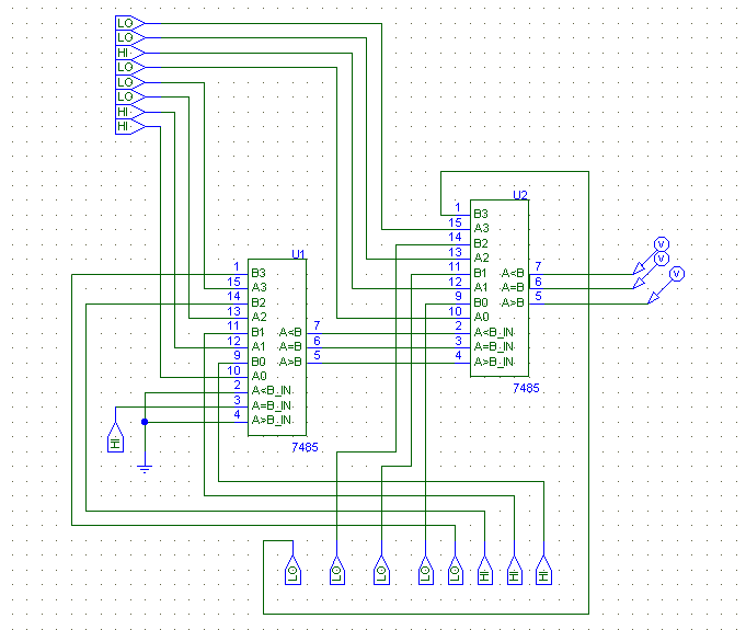
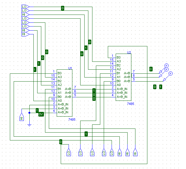
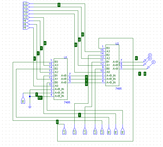
The first picture is the comparator design, the following three are the outputs in each of the three cases. In all cases, the top left bank of inputs is 'A', and the bank at the bottom is input 'B'.
Comparator Schmatic
A > B
A = B
A < B
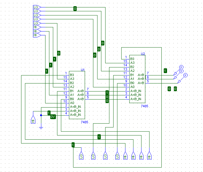
As can be seen from above, the comparator functions properly in all three modes. By connecting the output from A > B directly to the transistor relay, we will ensure that our Peltier Effect Cooler will only become active in the case where the Actual Temperaure is greater than the Set Temperature. When implemented, input B will come from a Debugger Board, while input A will come from the Thermistor via a Analog -> Digital converter.
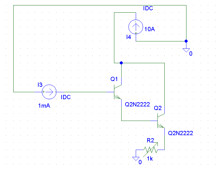
Back to the TopThe circuit is described as follows: The collector pins of both transistors are connected to a 10 A source. The base pin of the first transistor is connected to the output from our comparator circuit; the base pin of the second transistor is connected to the emitter pin from the first. Finally the emitter pin of the second transistor is connected to out load, in this case the Peltier Apparatus.
Here is the Schematic of our Transistor Relay
Here is the Simulation of the Above Schematic, as you can see we get the required 10 A output.
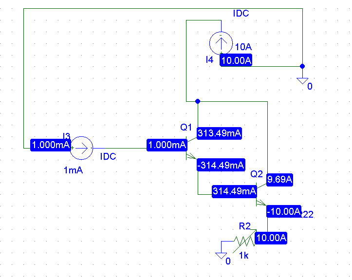
Although we are obtaining the desired output in the simulation, in practice we found that this configuration was not activating the transistors as we had hoped. We therefore decided to go with the modified design pictured below:
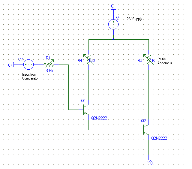
When implemented this design was found to work much better than the previous one, giving the desired output current when connected to our comparator circuit.
Back to the Top
We are planning to use a Programmable Logic Device to control our seven-segment displays. This will be accomplished by using the 8 outputs from the Analog to Digital converter as the inputs to the PLD, and by having the PLD generate 14 outputs to drive the 7 segments of each display. In our design, only 15 of the possible 256 intervals output from the Analog to Digital converter will be used, each corresponding to a specific temperature in degrees. We plan to configure our PLD basically at first, and then refine the program once the rest of the circuit has been implemented.
Here is the VHDL code we used to power our two seven-segment displays:
LIBRARY IEEE;
USE IEEE.std_logic_1164.all;
use IEEE.std_logic_unsigned.all;
ENTITY jeff IS
	PORT(temperature : in std_logic_vector (7 downto 0);
		 clk         : in std_logic;
         display     : out std_logic_vector (13 downto 0));
END jeff;

ARCHITECTURE interior of jeff is

BEGIN
	PROCESS (clk)
	BEGIN
		if (rising_edge(clk)) then
			case temperature is
				when "00000000" => display <= "10110111001111"; --23
				when "00000101" => display <= "10110111011011"; --22
				when "00001010" => display <= "10110110000110"; --21
				when "00001111" => display <= "10110110111111"; --20
				when "00010100" => display <= "00001101100111"; --19
				when "00011001" => display <= "00001101111111"; --18
				when "00011110" => display <= "00001100000111"; --17
				when "00100100" => display <= "00001101111100"; --16
				when "00101000" => display <= "00001101101101"; --15
				when "00101101" => display <= "00001101100110"; --14
				when "00110011" => display <= "00001101001111"; --13
				when "00110111" => display <= "00001101011011"; --12
				when "00111100" => display <= "00001100000110"; --11
				when "01000001" => display <= "00001100111111"; --10
				when "01000110" => display <= "01111111100111"; --09
				when others     => display <= "11110011111001"; --EE
			end case;
		end if;
	end PROCESS;
END interior;
When compiled in MAXPLUS, this code generated 0 errors, and 0 warnings.
Back to the Top
In order to 'Balance' our Thermistor, so that 0 volts were being output when the thermistor was at room temperature, we needed to construct a bridging circuit. The thermistor we are using has a listed base resistance of 20 ohms, for this reason we constructed the bridge using 20 ohm resistors. As can be seen in the diagram, we are planning to connect the bridge to our Operational Amplifier in a differential configuration (ie, connect two input voltages and take the difference). The inputs to the Op-Amp will be the two sides of the bridge, which side corresponds to positive and which to negative will be determined after the bridging circuit has been constructed.
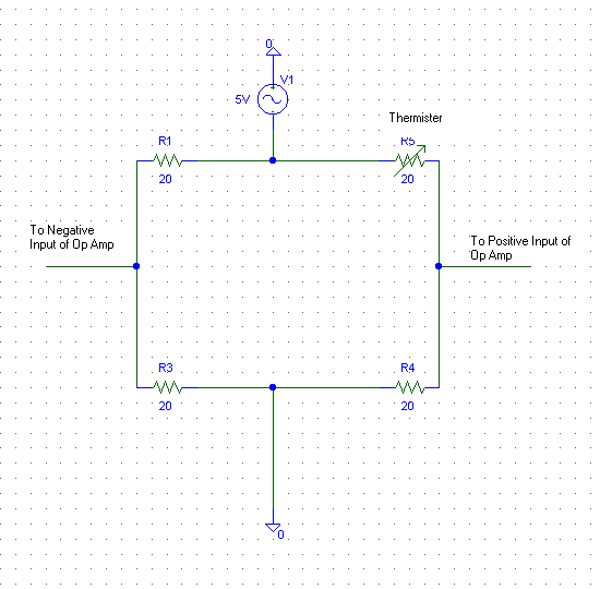
It should also be mentioned that in our configuration, as the temperature of the thermistor decreases, we are expecting the output voltage from the bridging circuit to increase, whereas when the temperature of the thermistor increases, the voltage should then decrease. We are also planning to have quite a substantial gain, since our thermistor will more than likely only change by a very small margin, probably around 0.5 mV for its entire range.
Back to the Top
The final section of our circuit is the Operational Amplifier (LM341), which was connected to our Analog to Digital converter (ADC0804). First, the Op-Amp. As was mentioned in the previous section, the output of the bridging circuit was quite low, thus we needed an Op-Amp with a built in gain, for this application we chose a closed loop gain of 10. Since we were dealing with two inputs (the positive and negative sides of the bridge), we needed to construct a differential amplifier which would amplify the difference of the two inputs. The circuit we implemented was constructed according to the following picture:
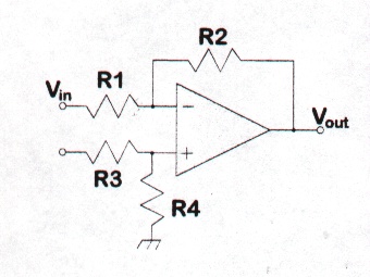
The amplification is governed according to the formula:
R2/R1 = R4/R3 = Gain.
Now, for the Analog to Digital Converter. This was a fairly simple portion of the project, since the converter was wired in the same manner as in the 'Digital to Analog and Analog to Digital' lab. The wiring was identical to the following diagram:
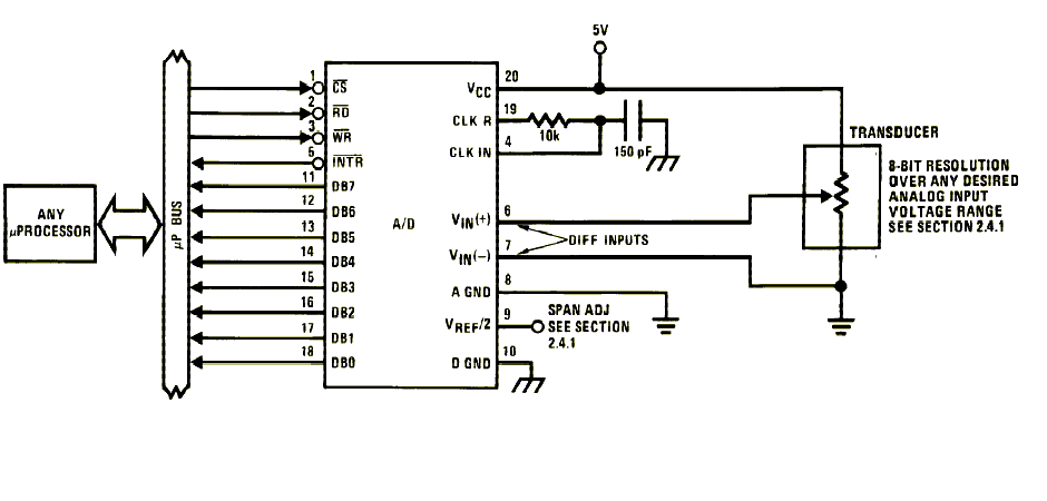
All digital grounds in the diagram (pins 10, 19, and 4) were considered to be analog grounds. The 'Vref/2' on pin 9 was accomplished with the aid of a 2 1/2 volt diode.
Back to the Top