 |
||||||||||||||||||||||||||||||
|
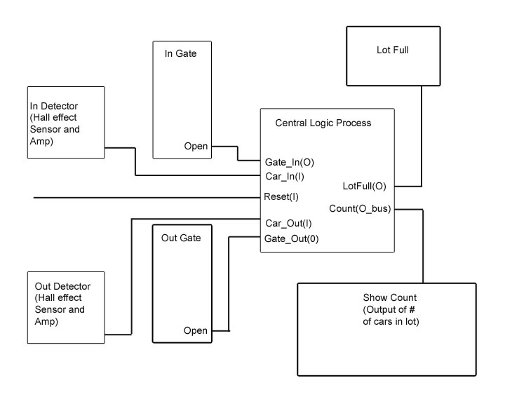
The Car Lot Management System is a circuit designed to manage a gated parking lot. The lot has a separate entrance and exit, each with a gate to allow cars to enter and exit. The circuit is customized for the size of the lot and will only allow enough cars in to fill the lot. Both the entrance and exit contain sensors which will detect the magnetic fields generated by cars and use these inputs to drive the system. These inputs are passed to the Central Logic Process where the inputs are compared with the number of cars in the lot, the present state of the gates, and a few other factors to decide whether or not to allow the car to enter/exit. The Central Processor will then drive the appropriate gate to open/close as well as output a new count of the number of cars in the lot. When a car is being let in or out the gate will stay open for a set length of time (which can also be adjusted easily). Along with the counter display you may also have a separate signal that is triggered when the lot is full. The figure below is a block diagram for the system, showing the main functional locations of the circuit.
|
||||||||||||||||||||||||||||||
| Back
to top
This section will show the different inputs and outputs of the circuit, it will also give a model test output in the form of waves. The table below summarizes the inputs and outputs.
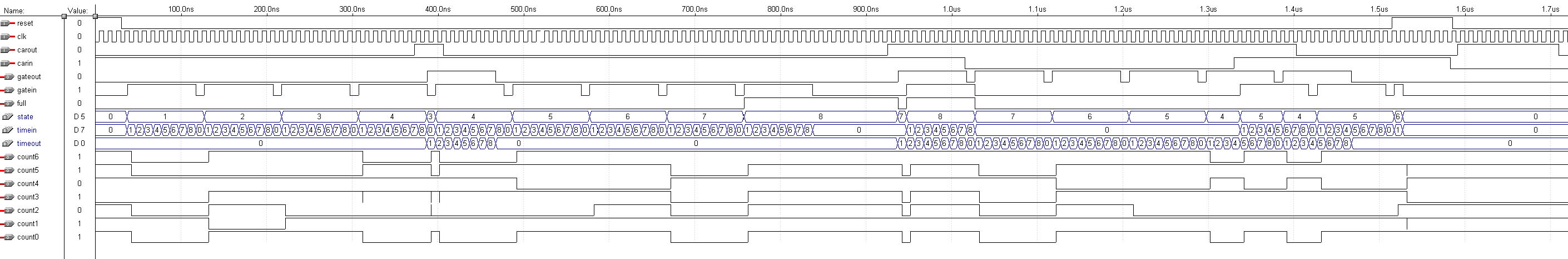
The timing diagram shows how the inputs and outputs are related. For this demonstration the lot size is 8 cars and the gate is delayed 8 clock pulses. Both of these numbers can be adjusted for the specific lot being managed. The timing diagram also contains the signals State, timein, and timeout. State is just a count of how many cars are in the lot, while timein and timeout represent how long their corresponding gate has been open. View the diagram here.
|
||||||||||||||||||||||||||||||
| Schematic
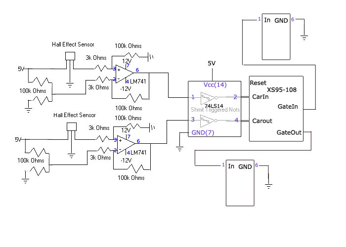
Below is the schematic diagram for the system. It includes all of the parts used to build our prototype. The inputs are created using Hall Effect Sensors and LM741 Op Amps. These are then fed through a 74LS14 Schmitt trigger, which converts the inputs to a more traditional digital input with an acceptable range for our CMOS CPLD. The Central Logic Process is created from a XS95-108 Prototyping Board with 5V, 2,400-gate CPLD . The two gates are represented by relays. All the resistor values are included in the diagram. Also, pin numbers are shown in blue text. No pin numbers are assigned to the CPLD because those are assigned by the user when programming the chip.
The Central Logic Process has been programmed into a CPLD. The actual unit has been designed using VHDL and then programmed into the chip. The code for the chip is included here. The original approach to designing this chip was as a state machine. However, this proved to be extremely difficult because of the number of inputs and outputs which would be required. Also, this made the design very difficult to modify for larger lots. The approach we eventually came up with was to use a combination of logic on the inputs and signals, then using the results to drive a much simpler process. Once the logic was worked out the design became much easier and is easily adapted to larger lot sizes. The logic that drives the 7 segment display is not perfect because it has a couple of static and dynamic hazards. However, these last only nanoseconds and since it is used only for a display they will have no effect.
|
||||||||||||||||||||||||||||||
| Prototype
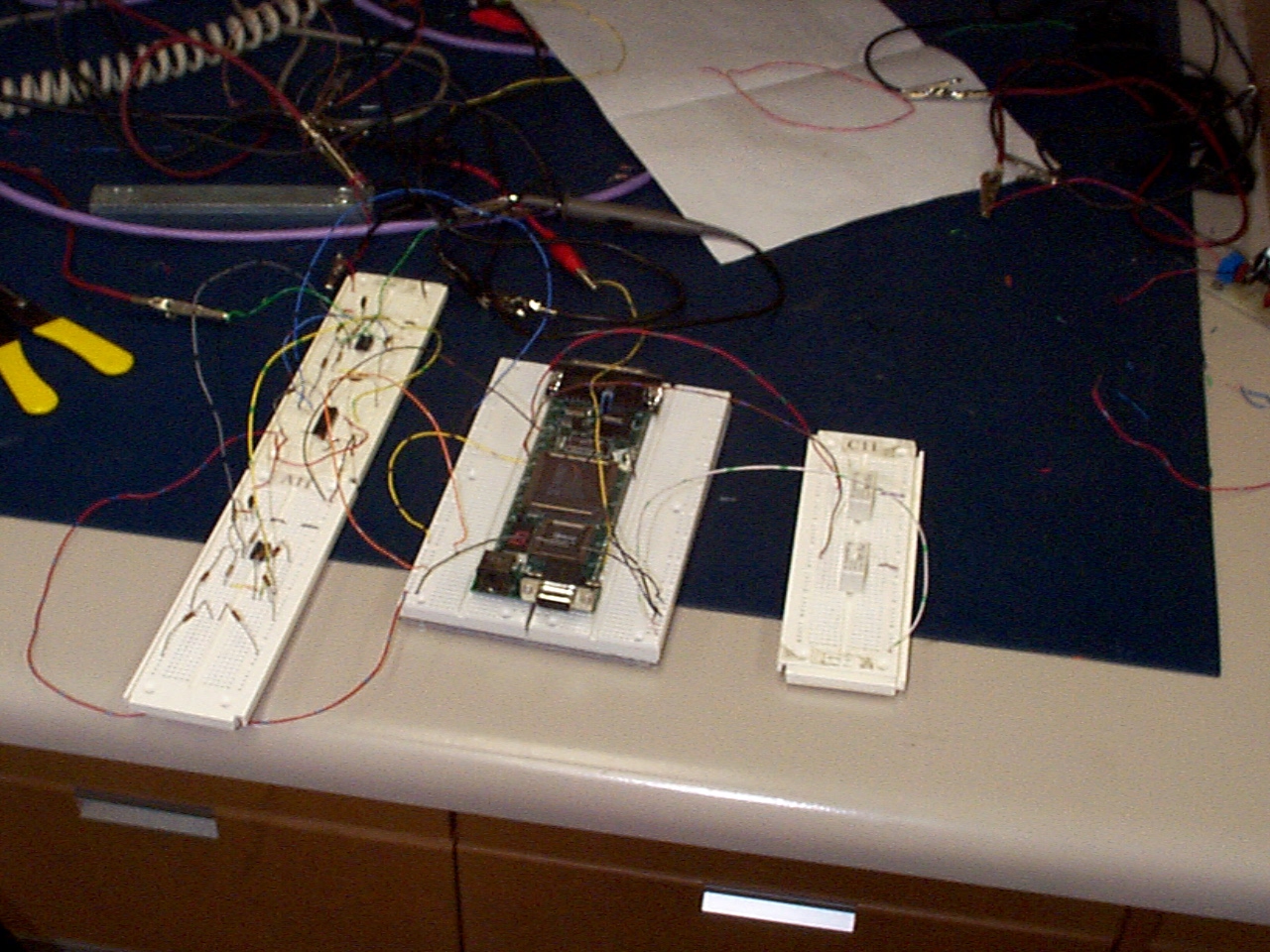
We built our prototype using the a system like the schematic diagram above, the differences are described below. We built each section separately and tested it extensively before connecting it to the other sections. We had to make several design changes during this process and ran into some difficulties. The inputs were built to the specifications above. We were not getting enough of a drop from the hall effect sensor so we decided to increase the ground on the Schmitt Trigger using two diodes. This gave us the operation we expected from the system. To operate the system you simply bring the south side of a magnet close to the Hall Effect Sensor. This causes the voltage to drop, the effect is amplified by the Op Amps and then fed into the Schmitt Trigger. The trigger is very similar to a NOT gate, except is uses different voltage levels (which make it compatible with CMOS), as the voltage drops the output from the Schmitt trigger goes HIGH. When the magnet moves away the opposite occurs. The CPLD gave us a lot of trouble. The first two boards we received were impossible to program and when we finally discovered the test software on the computer they both failed. We then programmed a third board, which finally gave us success. We tested the programmed board and everything worked perfectly, however the next morning the board had died for no obvious reason. After programming a fourth board, we finally had a working Central Logic Process Section. The operation was as expected from the timing diagram shown earlier. We used a 2 Hz clock to allow the changes to be more easily demonstrated. For our outputs we did not have the needed solenoids to build a working gate, so we showed the gate outputs from the CPLD worked properly by connecting relays to them. This was the easiest section of the board to design since each relay required only 2 wires. The relays click when voltage is applied and again when it is removed. This would allow us to tell when the gates are opening (voltage goes high) and then closing (voltage drops low again). Now it was time to connect the sections to get a complete system. Here we came across a new problem. The outputs worked perfectly with the Central Logic Process, but did not work properly with the inputs. We experimented with this system and got it to work with one input only, even this operation was improper. The cause of the problem was one of our earlier design fixes. When we increased the ground on the Schmitt Trigger we also increased it's low state output. The High state was still defined well enough, but the low state had a voltage higher than that allowed by CMOS. The voltage was actually in the undefined range and the effects were unpredictable. This caused the system to work some of the time and not others. In fact we managed to get an unstable state with perfect oscillation. Something we probably couldn't have accomplished if we'd set out to do it. We unfortunately ran out of time before we could fix this problem, but have since discovered the fix for it. Our weakness was that we used 12V and ground for the Op Amps, this didn't allow the system to lower it's input as close to 0 V as we needed. By using -12V for our ground value we would be able to pull the voltage down low enough. We would then remove the two diodes from the ground on the Schmitt Trigger. These changes should fix our problems, although we might need to change a couple of our resistance values to fine tune the system. Finally, below is a link to a picture of our prototype system. You can see that the inputs, Central Logic Process, and outputs are all on their own breadboards. They appear in the order mentioned above.
|
||||||||||||||||||||||||||||||