
Last Modified: 11/24/2000
Memory is the part of a computer which temporarily holds data that the microprocessor uses. It can be implemented in various fashions, using latches, flip-flops, capacitors or other common electronic components. In practice, Memory comes imbedded in VLSI DIP, DIMM, or SIMM IC's. There are two main types of memory: RAM (Random Access Memory) and ROM (Read Only Memory). RAM can be both read from and written to, while ROM is traditionally hard coded and its contents do not change. Because a RAM's contents are lost when power is turned off, it is referred to as volatile memory. Typically, data is transported between the CPU and Memory through groups of embedded hardware lines called buses. There are three main kinds of buses, namely the address bus, data bus and control bus.
The address bus is a one-way connection over which the microprocessor sends an address code to memory. The "width" of the address bus is specified by the number of bits that it can handle. The more bits there are in the address bus, the more memory locations can be accessed. For example, with 32 bits you can access 232 = 4 294 967 296 memory locations.
In contrast, the data bus is a two way connection between the CPU and Memory over which data, instruction codes, or the results of operations can be sent. The width of the data bus is usually dependent on the type of microprocessor. For example, a 32-bit microprocessor will usually employ a 32-bit data bus, so that its words can be sent across it one at a time.
Finally, the control bus is used by the microprocessor to coordinate its operations and to communicate with external devices. Read, Write, and Enable signals are commonly sent over the control bus. Some CPUs have separate read and write signals, while others have only one signal. When a single signal is used, it is usually high to read, and low to write (control signals are usually active low). When two signals are used there is one for read and one for write, with only one of the pair being asserted during any particular signal. One must bear in mind that assert, in this case, means to bring to an active level.
A digital memory device is an integrated circuit with
Memory operations, such as reading and writing, can only be performed when the chip select(s) are asserted.
For a read operation to occur, the chip select(s) and the read signal must both be asserted. In that case, the value at the location specified by the address pins will be placed on the output pins. (If the address pins are floating, the output will be from some indeterminate location.)
For a write operation to occur, the chip select(s) and the write signal must both be asserted. In that case, the value on the input pins will be stored at the location specified by the address pins. (If the address pins are floating, the data will be stored at some indeterminate location. If the data pins are floating, then an indeterminate value will be stored.)
The basic write operation is illustrated below. To store a byte of data in the memory, a code held in the address register is placed on the address bus and selects the specified location in the memory (Step 1). Also at this time, the data held in the data register is placed on the data bus (Step 2). When the write command is detected on the control bus, the information on the data bus is written to memory (Step 3), overwriting whatever was previously held in that address location.
Figure 1. The Write Operation
The basic read operation is illustrated below. Again, a code held in the address register is placed on the address bus (Step 1), selecting the specified location in memory. The Control bus then passes on the read command (Step 2), and a "copy" of the data that is stored in the selected memory address is placed on the data bus and loaded into the data register (Step 3), thus completing the read operation. When the data is read from a memory address, it remains stored at that address and is not destroyed.
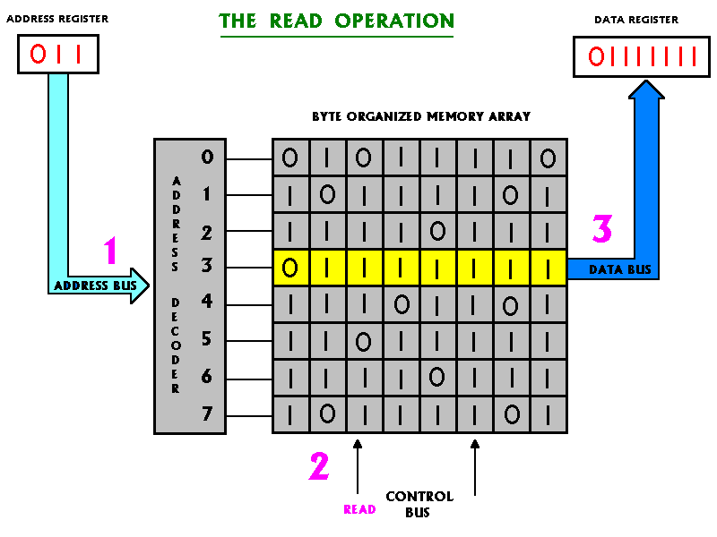
Figure 2. The Read Operation
If the width of the CPU's data bus is greater than the memory's data bus, then multiple memory devices will usually be used in parallel, so that the CPU's words can be stored in entirety.
If, however, the width of the CPU's address bus is greater than the memory's address bus, then the CPU's address bus must be decoded to divide the total possible memory space into manageable chunks, small enough for the individual memory devices. The chip select(s) for each device are wired so that the CPU doesn't notice the difference. If there are not enough memory devices to cover all the possible memory locations, than ghosting can occur (the same data appears at different addresses). In this case, the CPU should be programmed not to use the excess memory locations, to avoid program errors.
The diagram below illustrates a first step in decoding the CPU's address lines so that ghosting can be avoided. Here, the CPU has 16 address lines, while each memory device has only 8. This means that the CPU could potentially address 216 = 65 536 locations, while each device only provides 28 = 256 slots of memory. A15 is tied to two memory devices' chip selects (to one as an active high control, to the other as an active low). This means that only one memory device will be active at a time (depending on the level of A15), so that the amount of memory available to the CPU is effectively double the capacity of a single device (512 locations). Note however, that lines A8 through A14 are still sources of ghosting, since their level (either high or low) does not alter the address location being accessed. These lines would also have to be decoded and tied to 254 other memory devices (to provide the CPU with the remaining 254 * 28 = 65 024 memory locations) in order to completely eliminate the possibility of ghosting.
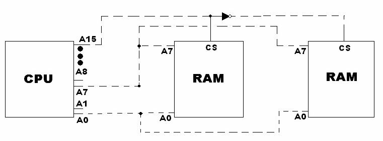
Figure 3. First step in resolving Ghosting
An I/O port provides an interface between the computer and the "outside world". The two ways in which I/O ports can be implemented are: Dedicated I/O ports and Memory Mapped I/O Ports.
With a Dedicated I/O port, the I/O port is given an unique address within the I/O address space of the computer. Dedicated I/O commands are most often used for communication.
Another approach to accessing I/O ports is the memory-mapped port. Memory-mapped ports are assigned addresses within the computer memory address space and are actually viewed as memory locations by the CPU.
An Input Port for a CPU can be created by placing a tri-state buffer on its data bus, asserted only when a particular memory address is selected. In this way, when the CPU tries to read from this location, the buffer will allow external data to flow onto the data bus, and thus to the CPU. The CPU should be programmed not to write to this address.
An Output Port for a CPU can be created by placing a latch on its data bus, asserted only when a particular memory address is selected. In this way, when the CPU writes to this location, the latch will capture the data on the data bus, and store it for reading from outside the machine. The CPU should be programmed not to read from this address.
An Input/Output Port is simply a combination of the above, where the choice of which way to function (input or output) is controlled by CPU signals (on the control bus). Usually the input and output pins for such a port are combined and are simply called data pins. In this case, the pins will be tri-state, meaning they can be high, low or high impedance (floating). On read operations, they contain the data to be read from the port, and on write operations they float so that the CPU may determine their state. When the CPU is interacting with other memory locations, they also float, so as not to interfere with the computer's operation.
Further Reading
Digital Fundamentals, 6th Edition: Floyd, Thomas L. Prentice Hall, 1997. (PC120 Text)
Chapters 12 and 13 of this text contains a very thorough explanation of all the topics discussed above.
Structured Computer Organization, 4th Edition: Tanenbaum, Andrew S. Prentice Hall, 1999. (CP216 Text)
Sections 2.2, 3.3 and 3.36 of this text contain great insights into memory operation.