Group: Ursula Emblau, Chris Thompson and Robert Carroll
References: The information on this page was taken exclusively from Terry Sturtevant's lecture notes and Fundamentals of Linear Circuits by Thomas L. Floyd. Images with Figure 13-xx are taken from the text and additional information is available in those sections.
The background for this site was taken from the Datasheet for National Semiconductors DAC0800/DAC0802.
Data sheets for A/D and D/A converters can be downloaded from: National Semiconductor
I. Digital to Analog Converters
A Digital to Analog converter will convert a digital signal in to its analog equivalent.
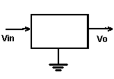
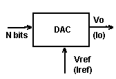
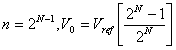
A. Function
Vo is the analog output voltage
Vref is the reference voltage
N is the total number of bits of digital data permissible
![]()
![]()
![]()
Modes
B. Parameters
![]()
where N is the total number of bits. This value is usually expressed in percentages.
![]()
where Vo is the output voltage, Vs is the source voltage and it is usually expressed in percentages. An ideal converter would have 0% power supply sensitivity.
C. Interfacing
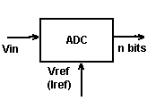
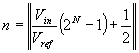
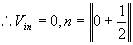
II. Analog to Digital Converters
Analog to Digital converters will convert an analog signal into its digital equivalent.
A.
Function
Vin is the analog input voltage
Vref is the reference voltage
N is the total number of bits of digital data
n is the number of bits in the output

B. Parameters
![]()
where Vo is the output voltage, Vs is the source voltage and it is usually expressed in percentages. An ideal converter would have a 0% power supply sensitivity.
C. Interfacing
A Tri state output is a feature of some digital electronic devices which allows a connector (pin) to either act as a normal output, driving a signal onto a line, or to be "tri stated" - set to a high-impedance ("high Z") condition. This allows other outputs to drive signals onto the line. Often the same connector also functions as an input when its output circuitry is tri stated. Tri-state outputs are typically used for the connection of several digital circuits to a shared bus onto which any one of them may output data for the others to input.
III. Voltage References
Conversions can be very sensitive to supply voltage changes, especially high resolution or many bit conversions, so it may be very important to have a known, and stable supply. Often immediately available sources, such as hydro outlets, will not provide a precise or stable voltage and a voltage reference device must be used.
A. Single Chip
- Very low sensitivity to power supply (~2ppm/v)
- Very low temperature coefficient (~1ppm/0C)
- High initial accuracy (~0.01%)
B. Zener Diode
- Readily available
- Cheap
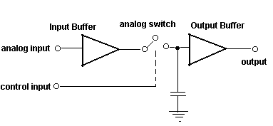
IV. Sample and Hold Amplifiers
A sample-and-hold amplifier samples an analog input voltage at a certain point in time and retains the sampled voltage for an extended time. This process enables the analog signal to remain constant for the amount of time required to convert it to a digital signal by the Analog to Digital Converter.
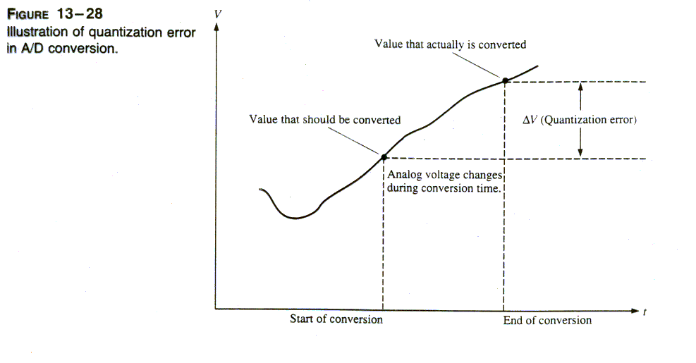
A quantization error occurs when there is a change in the analog signal during the conversion time. This error depends on the frequency and amplitude of the signal and the resolution needed for the digital output. If the quantization is going to cause error in the digital signal it must be addressed.
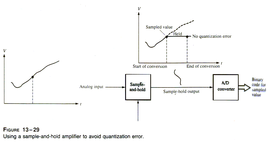
A sample-and-hold device, as the name suggests, samples the analog signal when the conversion starts and holds it for the duration of the conversion, eliminating the quantization error.
A. Function
B. Parameters
C. Uses
This circuit is used in Analog to Digital and Digital to Analog Converters.