PC/CP300 Electronics Laboratory II
Digital-to-Analog and Analog-to-Digital Converters
Objectives
Interfacing between analog input devices and the typically digital processing environment, e.g. microprocessor or embedded system, requires analog input signals to be converted to digital signals for processing. The results of the processing then have to be converted to analog signals for controlling analog output transducers. These conversions are done by analog to digital (A/D) and digital to analog (D/A) converters, respectively. Although you could construct these converters from discrete components, integrated circuits specifically designed for these purposes are usually used. The objectives for this lab are:
- to test the D/A and A/D ICs for proper operation
- to investigate the characteristics of the D/A and A/D converters
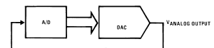
At completion of the lab, you should have both an A/D circuit and a D/A circuit on one breadboard. One of the configurations you will be using in this lab is shown below. Use this as a guideline for positioning the circuits on the breadboard.
Do not dismantle the A/D and D/A circuits. Store these circuits in your lockup area for use next week.
Preparation
| Great care should be taken to avoid static discharge into CMOS based chips. |
Before starting the lab, review the CMOS handling procedures.
- Always use a ground strap. If your grounding mat doesn't have two grounding straps, one for each of the partners, see the lab instructor.
- CMOS devices should be stored pin down in conductive foam when they are not in a circuit.
- Never leave unused inputs floating; connect to ground or +5V to prevent excessive current consumption and erratic behaviour.
- Never connect an input signal to a CMOS device when the power is off.
Equipment
- bench supply, oscilloscope, function generator
- breadboard, debugger board, resistors, capacitors
- DAC0800 [PDF: 11 pages], a digital-to-analog converter from National Semiconductor
- ADC0804 [PDF: 41 pages], an analog-to-digital converter from National Semiconductor
- LM 336-2.5 2.5 V zener diode [PDF: 12 pages]
- LM 336-5.0 5.0 V zener diode [PDF: 11 pages]
Procedure
Zener diode references
NOTE: For both the DAC and the ADC, you will need to use a zener diode circuit with a diode that is appropriate for the reference voltage. Do NOT use a supply voltage by itself or a resistor based voltage divider for the reference voltage.
- Look at the data sheet for the LM336-5.0 Zener diode.
Find the following parameters:
- Operating current range
- Nominal voltage
- Dynamic impedance
- Pick a current value near the logarithmic centre of the operating range, and use this and the nominal voltage to calculate an appropriate series resitor to use with a 12V supply.
-
Do not connect the adjustment pin for anything in this lab.
Use a convenient resistor close to what you calculated and connect it to the Zener diode and 12V supply. Measure the output voltage to see that it agrees with expectations. - Now replace the 12V supply with the function generator. Set the output to a 1V sine wave with a 12V offset. This will allow you to see how much the reference voltage changes with changes in the supply voltage.
-
Observe the voltage accross the zener diode for a few cycles of
the input. Sketch the output and identify the vertical scale to
show the size of the variation.
What is the ratio of the change in reference voltage to the change in supply voltage? (For instance, if the reference changed 0.2V for 2 V change in supply, that would be a ratio of 0.1.)
Demonstrate your circuit to the lab supervisor. Keep this circuit for future labs.
Digital to analog conversion
- Using a DAC0800, design a circuit to take in an
8-bit digital value and produce an appropriate analog output
between 0 and 5 volts.
The sample circuits shown in FIGURE 3. Basic Positive
Reference Operation and
FIGURE 9. Positive Low Impedance Output Operation
should be of use.
Demonstrate your circuit to the lab supervisor. Keep this circuit for future labs.
Analog Ground
 versus
 Digital Ground

Take careful note of the different ground symbols. For any circuit handling analog inputs that has a digital component, separate grounds must be used for the analog and digital portions of the circuit to avoid digital noise from getting into the analog input circuit.
* Use separate buses for the analog ground and the digital ground.
* Bring the grounds together at a single point as close to the power supply as possible.[Explanation of second sentence Note 2 on page 4 of ADC0804 data sheet.]
Analog to digital conversion
- Using the ADC0804, construct a circuit to convert
a 0-5 volt input signal to a digital value from 0 to 255 and
run the ADC in continuous or free running mode.
Construct the circuit on the same breadboard that was used for
the DAC circuit.
- How does this circuit compare to the Basic A/D Tester (Figure 9 on page 24 of datasheet)?
- For the circuit you built, what is the speed of the ADC internal clock? See, §2.6 Clocking Option and do the calculations.
- What relationship does this speed have to the number of clock cycles required to complete a conversion?
- Determine the smallest voltage change which can be detected by the circuit. Measure the change in voltage by slowly varying the input voltage and watching for the change in state of the LEDs.
- Is this change in voltage the same for input voltages over the entire 0-5 volt range?
- Are these results consistent with the
expected resolution of the ADC? Show the calculations.
- Explore modifying the input range by altering the
reference voltage.
For example, what reference voltage do you need to obtain an
input range of 0 to 2.5V.
Is the smallest change in voltage that can be detected by the
circuit
equal to ½ of what it was with the input range of 0-5
V?
Demonstrate your circuit to the lab supervisor. Keep this circuit for future labs.
Combination
- Combine the DAC and ADC circuits by using the
ADC output lines to drive the DAC0800 as shown in the
figure below.
Warning: carefully check for the most and least significant
bits when connecting the digital lines;
the numbering of the bits is not consistent.
Drive the ADC input with a sine wave of the appropriate amplitude. Compare the analog output of the DAC with the original sine wave and sketch the signals.- How high a frequency can this system accept before the output becomes too distorted?
- What part of your system dominates this frequency limit?
A square wave input might make seeing where the output
deviates from the input easier.
Demonstrate your circuit to the lab supervisor.


