PC/CP220 Digital Electronics Lab
Introduction to Quartus II Software
Design using Test Benches for Simulation
(Note: If you have done the previous task which involves
"forcing" the
inputs for simulation, the first several sections of this document are
identical. If you saved your previous work, you can skip to the testbench
section where the changes begin.)
In this tutorial, we will show
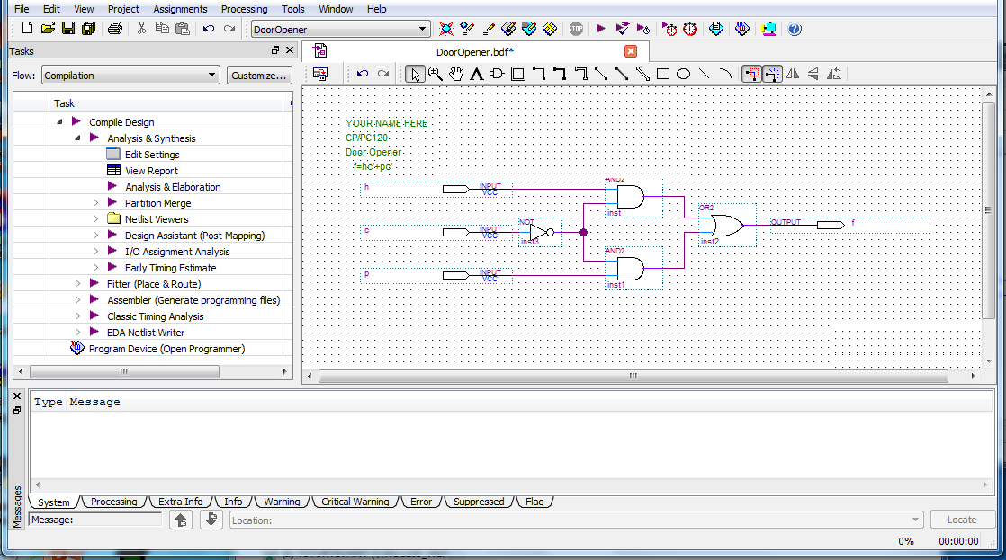
you how you capture the schematic design for the automatic door opener circuit
using Altera Quartus II software.
The Problem
We are designing a circuit for an
automatic door like those you see at supermarkets. The door should
open only when a person is detected walking through or when a
person presses a switch (such as the wheelchair button) to have
the door open. The door should only operate if it has been unlocked.
- output: f = 1 (Opens Door)
-
inputs
- p = 1 Person Detected
- h = 1 Switch Holding the Door Open
- c = 1 Door Closed/Locked
- Want door to open when
- the door is unlocked and person walking through (c=0 and p=1)
- the door is unlocked and the switch is set to hold it open
(c=0 and h=1)
I: Drive
During Labs you will need to save all your work under a
directory called
CP220 in your Home Directory (drive I:)
To get to your I: or your Home Directory double click on My Computer icon on
the desktop.
Under I:\CP220 create the following folders

Copy this directory from the I drive to the E
drive. There are currently probelms saving files directly to the I
drive. Be sure to copy your files back to the I drive after you are
done.
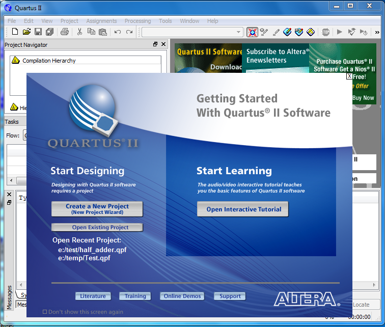
Getting Started with Altera Quartus
Launch the Altera Quartus software. You should see a screen such as
this:
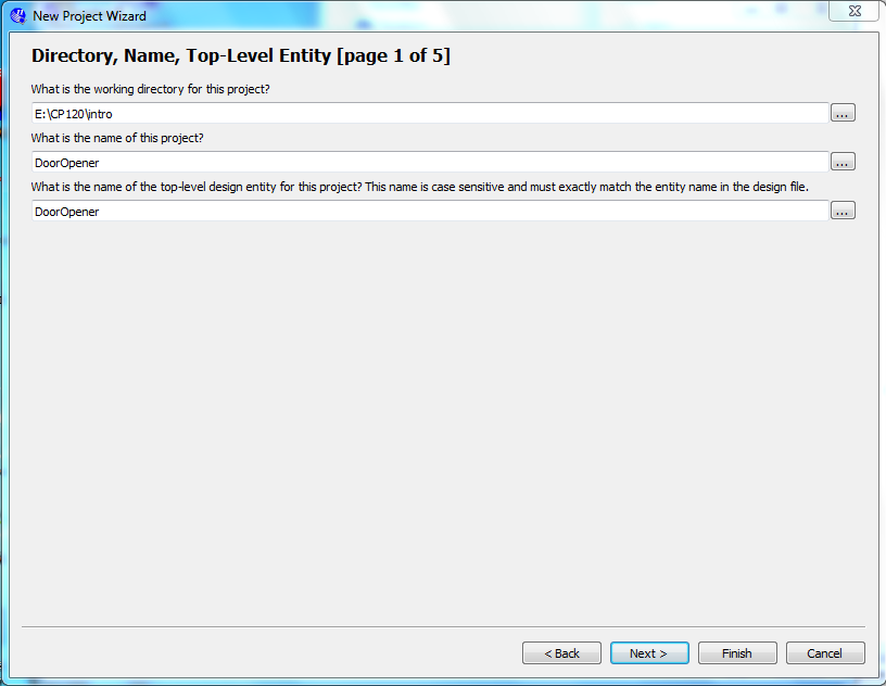
Creating a New project
Select the
File →
New Project Wizard; a window like the following will
appear.
To select the working directory use the button to browse and
select
E:\CP220\intro.
Name the project DoorOpener.
(Note that the next field gets filled in automatically.)
Select
Finish.
Don't uses spaces in file or directory names.
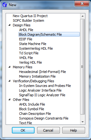
Creating a new Schematic design
Select File
→ New -
A window as seen in the following picture will open.
Select 'Block Diagram/Schematic
File' and press OK.
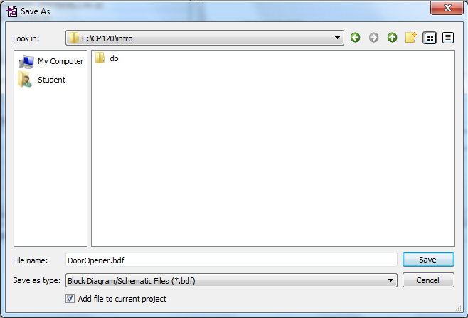
This should open a palette where you
will design your circuit. This palette is designated Block1.bdf. Save this
graphic design file as DoorOpener in your "intro" directory. The file
will be
given the bdf extension; bdf stands for block design file and contains
schematics, symbols or block diagrams.
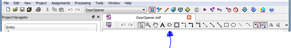
Adding text
- Select the A below the arrow to the
left of your Block Diagram/Schematic File window (also known as the
palette).
- Select a point near the top left in
the window with the left mouse key.
- Type your name and then hit the
Enter key.
- Type your project name and then hit
the Enter key.
- Type the following equation,
f = hc' +
pc'
, and then hit the Enter key.
- Hit the Esc (escape) key to end
text additions.
Adding a Component
- Click the
library icon.
The Symbol dialog
box will appear. This window lists the available Altera libraries as seen
in this image.

- Expand the /altera/quartus10.0sp1/quartus/libraries
folder, expand the primitives folder and then expand the logic folder.
- In the logic folder, select the
and2 component by double clicking on it (or by selecting it with a single
click, then selecting OK).
- Click the pointer at the desired
location in the Block Diagram/Schematic Editor window to
insert the AND symbol
into the design file.
Repeat these steps to enter
an OR (or2)
gate and a NOT (not) gate.
(If you wanted to add multiple NOT
gates, you could select the Repeat-insert mode box.)
In the same manner that you placed a
gate onto the palette, add three input pins and one output pin from
the Symbol libraries. Input
pins can be found under primitives | pin | inputs. Output
pins can be found under primitives | pin | outputs.
Name your input and output pins as you name them in your equation. Double
click on the pin name to change its name.
Rearrange your devices in approximately the placement you would like
for the
logic diagram you are trying to construct. You can move a component
by selecting
it with your mouse, holding down the left button and moving it to another
location on the palette.
Save your design. It is a good
idea to save your design often, just in case something bad happens .
Save the bdf file with the same name as the project.
Don't use spaces in any file names.
Wiring your circuit
Select the orthogonal node tool.  Place your pointer on the output of one of the input pins and
hold the
left mouse button down. You should see a cross-hairs or + appear at the
output.
Place your pointer on the output of one of the input pins and
hold the
left mouse button down. You should see a cross-hairs or + appear at the
output.
Drag your pointer to the input of the AND gate. Every time you release the
mouse key, the line (wire) ends. If your wire did not reach the AND gate, you
can add to the wire by putting your mouse over an end of the wire and again
selecting it with your left mouse button and dragging your mouse to another
position.
Don't run wires along the edge of a device. This
can cause simulation problems.
Don't leave inputs and outputs right next to the
chips. Make sure you can actually see some wire between them, otherwise
you may have simulation problems.
Note: Make sure you do not make the wire too long. If you drag it
too far you will see an x; and this is considered an open
connection and your design will not compile.
To delete a wire or a portion of a wire, simply click on it (it
should change
color to indicate selection) and press the delete key.
If wires are connected to the component as you are moving it, the wires will
drag and stay connected to the component. This is referred to as "rubber
banding" and is a feature of all major schematic entry design packages.
(You can turn rubberbanding on and off using the rubberbanding tool. )Add the
rest of the wires needed to connect the logic diagram.
)Add the
rest of the wires needed to connect the logic diagram.
The window should look something like image below.
Save your
design.
Printing
We will not print today. But you will need to know how for your project.
To print, go to File | Print. If you want to
change what appears on the
printout or how it appears, go to File | Page Setup
change print settings.
Before printing, you can view what the print will look like by
selecting File |
Print Preview
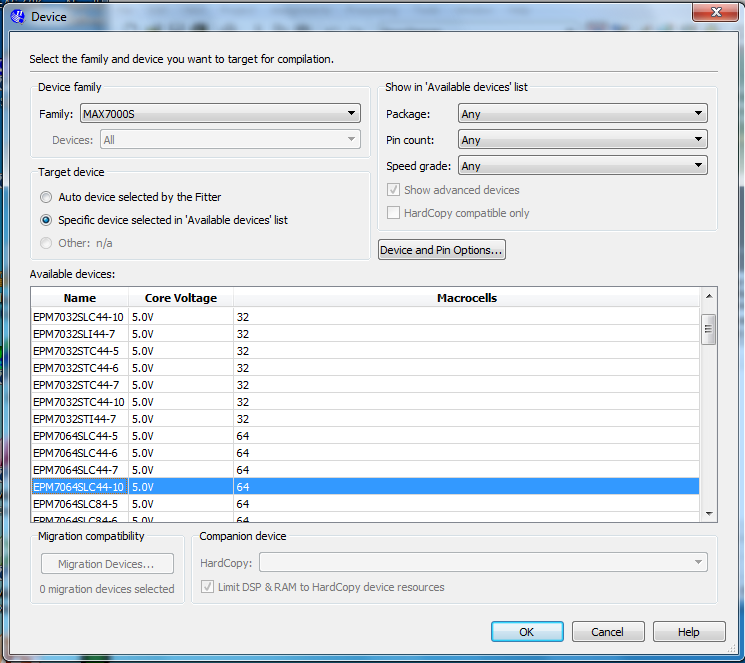
Choosing a Device
The programmable device which we'll use for our design can be chosen now.
Select Assignments | Device from the pull-down menu.
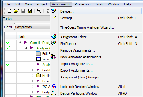
Select MAX7000S from the "Family" pull-down list.
Select the "Specific device selected" and then choose
EPM7064SLC44-10,
which is the device we are using in our lab. Select "OK."
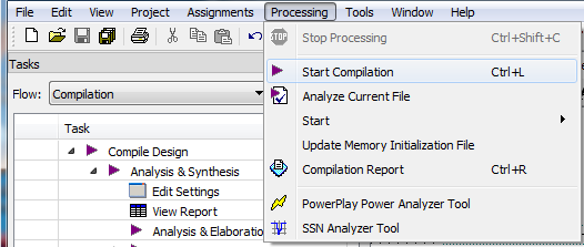
Circuit Compilation
You will need to compile
your design to ensure you do not have any errors in your circuit (e.g. you do
not have any open connections, etc.)
Click on Processing | Compiler Tool to
start compilation. Then click start.
Circuit Simulation
Before simulating, some preparation is required.
Configure NativeLink settings:
- NOTE: This is DONE ONCE PER PROJECT and the information is
stored
with the project information.
- Select Assignments | Settings.
The Settings dialog box appears.

- In the Category list, select EDA Tool Settings | Simulation .
The
Simulation page appears.
- In the Tool name list, select ModelSim. [Do not turn on
Run
gate-level simulation automatically after compilation.]
- Format for output netlist should default to VHDL and the output
directory to simulation/modelsim. [Select/enter if necessary.]

- Select More EDA Netlist Writer Settings and change the
following
options:
- Turn ON Generate netlist for functional simulation
only.
- Enter the Location of user compiled simulation library,
e.g.
C:/MSim_lib [if necessary].
- Select OK.

- Select More NativeLink Settings and change the following
option:
- Enter the Location of user compiled simulation library,
e.g.
C:/MSim_lib [if necessary].
- Select OK

Convert the schematic diagram into VHDL code for
simulation.
- ModelSim requires that the system be specified in an HDL
(Hardware Definition Language); we will
be using VHDL
- Have the schematic open and then select
File | Create/Update |
Create HDL Design File from Current File.

- In the pop-up window, select file type as VHDL
and the file
name will show the name and path of the file.
The VHDL file and the BDF file have the same name
but
different extensions (for example, if your BDF file
is example.bdf, the VHDL file created is
example.vhd).

Add the VHDL file to the project and
compile for simulation.
- Open the VHDL file using File | Open.
Then add it to the project
using Project | Add Current File to Project.


+ Note: The VHDL file has three parts:
- the library definitions including work where
your project will be stored,
- the entity definition which is a
wrapper that defines the
inputs and outputs to the design component,
and
- the architecture which defines what your
component does.
- Remove the BDF file from the project
(system can't handle two source
files for the same circuit) by selecting
Project | Add/Remove Files in Project
and then selecting the BDF file and
Remove.
Note that this does not delete the file (and we
do not want to delete the file).
(You don't even need to close it.)


- Compile the circuit for a functional simulation by selecting
Processing | Start | Start Analysis &
Elaboration.

Library Compilation
It may be necessary to compile the libraries for your device family
before you simulate.
Click on Tools | Launch EDA Simulation Library Compiler.

The MAX7000S family should already be selected, so
click
Start Compilation.

Don't worry if you get any error messages.
Create a testbench to automate your simulation.
- You can get Quartus to produce a shell testbench
file by selecting
Processing | Start | Start
Test Bench Template Writer.

There will now be a file in your
simulation\modelsim directory.
Open it.

- The section near the bottom of the file is where
you put statements for your simulation.

Insert instructions for how you want the inputs to change through the
simulation.
Here's an example of the beginning for a very simple simulation:

- After making the changes, you need to change the settings
to include your testbench.

Choose a New testbench.

Give the test bench a name. It doesn't have to be the same as the
file name.

Now add the testbench file.

Select OK to close the New Test Bench Settings window..

Select OK to close the Test Benches window..

Select OK to close the Settings window..

- Select the VHT file.
Then add it to the project
using Project | Add Current File to Project.
- Prepare for a functional simulation by selecting
Processing | Start | Start Analysis &
Elaboration.
Launch the ModelSim simulator.
- Select Tools | Run EDA Simulation Tool |
EDA RTL Simulation.
ModelSim will display splash screen. ModelSim will
load libraries and compile the project.
The transcript pane at the bottom of the screen
indicates the scripts
that have been run (or are running).

- Now your work library will
contain two VHDL files; your circuit and your
testbench. Select both,
and right click to compile both.

- Select Simulate | Start Simulation to put
ModelSim in simulator mode.
The Start Simulation Window opens.

- The Start Simulation window contains many tabs.
The Design tab lists the designs available for
simulation; most are system libraries.
At the top of list will be work (default name for the
library containing your program),
expand work by selecting the '+'.
All components in your design will be listed, select
the component that is the testbench.

Select OK.
This will bring up other panes.
- Then the left hand side of the screen should now contain a
sim tab that displays the design units in your circuit
and the supporting libraries.
When a design unit is selected in the sim tab,
the corresponding signals are shown in the objects
window on the
right hand side of the screen.
Signals that are preceded with a plus (+) sign indicate
a bus (a group of wires with common function).

Open waveform window and add signals to be simulated.
- For each signal that you want to add to the simulation,
right click on the signal name in the Objects window
and
select Add | To Wave | Selected Signal.
Typically, you would want to add all inputs and
outputs.
A waveform window will appear in the work area.

- Alternatively, you can add a range of signals at
once by
selecting the 1st signal and then, while holding down
the shift key,
select the last signal in the range.
Then right click in the selected signal region and
select Add | To Wave | Selected Signals.
A waveform window will appear in the work area.

- When all signals are selected, expand the Wave
window.
- If the Wave window is not floating above the ModelSim
main screen,
use the top left icon in the wave window to undock the
window. Expand the detached window.

- In the tool icons, find the window that contains
the period of the signal,
e.g. 100ns. Immediately to the right of that window
will be the
run simulation icon (looks like a page with a blue
down arrow beside it).
Select run simulation.
You should see the inputs that you entered and the
outputs from your system on the waveform.
The period of the run will correspond to the time in
the period window.
All signals should be green.
If any signals are red, then
one or more of the inputs was not specified.


- The output can be zoomed.


-
To zoom back out to see the original, you can go to
View | Zoom | Zoom Full.

- The waveform can be exported to an image file.

Demonstrate the circuit to the lab
demonstrator before you leave.
Copy your directory from the E drive to the
I
drive. Delete them from the E drive
and empty the Recycle Bin so they don't get used by
someone else later.


