Pages created and updated by
Terry Sturtevant
Date Posted:
November 20, 2018
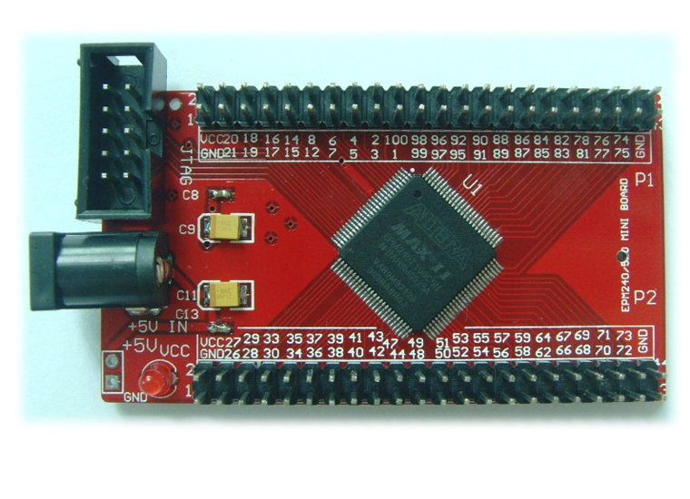
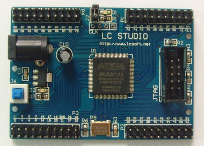
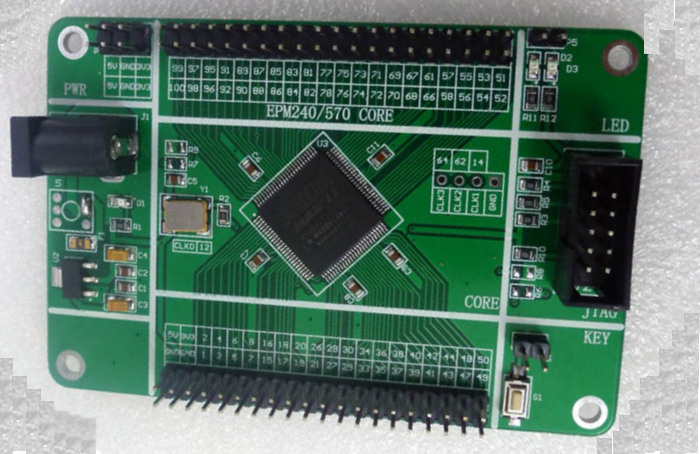
This CPLD has a lot more I/O pins than the EMP7064. This allows much
more complex circuits to be programed into it.
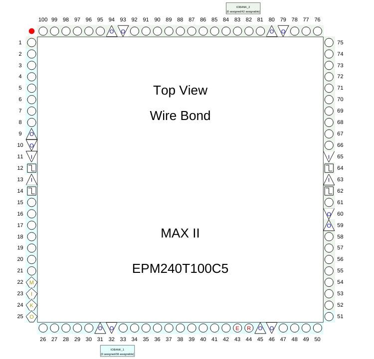
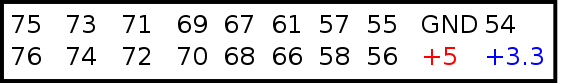
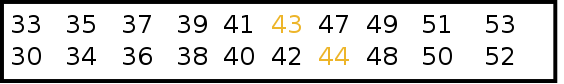
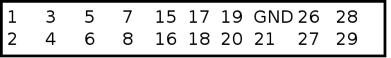
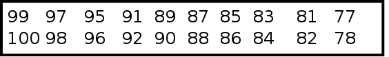
Note that there are about 80 I/O pins on the device.
One of the other things about this chip is that is is based on 3.3V
logic, not 5V logic.
This means that you will only use a 3.3V power supply, rather than a 5V
power supply so that the chip doesn't get damaged by overvoltage.
The JTAG connector is polarized, so that it can only be
connected the correct way. (Note the notch in the JTAG connector, which
corresponds with the ridge on the JTAG cable from the USB-Blaster.)
Each of these boards has an on-board voltage regulator,
so they can be powered with a 9V adapter or battery.
Notice that the I/O pins are in banks. If you look at a bank,
though, you should note that the pins are not always in numerical order.
Because of this, when connecting inputs and outputs it will make sense
to assign pins in the order they appear on the banks, so that
it's
easy
to use ribbon cables to connect to the outside world.
Note that the order of pins will be different on each of these boards.
The idea is that if you are connecting to an external device, (or
devices), then if you order the pins in the CPLD to match the order on
the external device(s), then your cables simply need to connect 1:1.
Since the CPLD is a 3.3V device, you can't have any 5V
devices connected.
This applies to the debugger board.
However, the logic on the debugger board can also operate on
3.3V.
If the debugger board is powered by 3.3V from the CPLD,
then there will be no problem.
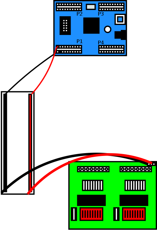
P1 has pins for 3.3V and GROUND.
Use P1 pins for +3.3V and GROUND to power the debugger board.
If your circuit only uses part of a CPLD, you may be able to
incorporate input and/or output circuitry inside the CPLD.
You could include a keypad encoder.
You could include a 7 segment display decoder.
This is easy because different circuits can be inside a single CPLD.
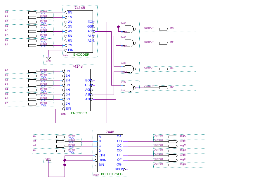
Notice that the input and output portions do not have to be
connected to each other in any way.


![]()
Wilfrid Laurier University
© 2019 Wilfrid Laurier University