PC/CP200 Electronics Lab I

Logic Gates Characteristics - Open Collector Outputs

Objectives

  1. To gain more experience with an oscilloscope.
  2. To investigate the operation of open-collector gates including the use of pull-up resistors.
  3. To investigate the operation of wire-ANDing.

Preparation

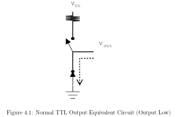
The current limits of normal logic gates are reduced with open collector gates (if using TTL) or open drain gates (with CMOS). The two types of gates are functionally equivalent, so it's only necessary to discuss one. The transistors at the outputs of a normal TTL gate can be thought of as switches, so that the circuitry looks as in Figure 4.1. The two switches are always in opposite states, so when the upper switch is open, the lower switch is closed and thus the output is low. (Actually, when the inputs are in the "undefined" region, the transistors are both in a state in between "open" and "closed", and so could be thought of as resistors of some finite value. However we will only discuss the "normal" cases.)

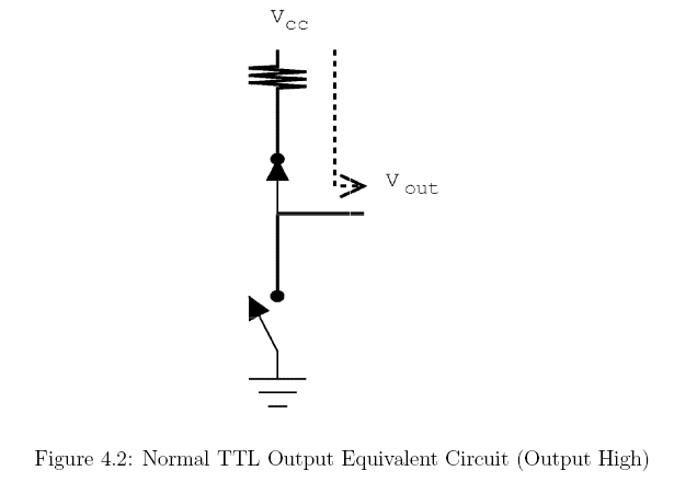
You will note in this case that the device will be sinking current, as indicated by the arrow into the device.

ttl output

If, on the other hand, the upper switch is closed, and the lower switch is open, so that the circuitry looks as in Figure 4.2, then the output is high (because it is connected to Vcc through the pull-up resistor.) In this case, the gate is sourcing current, as indicated by the arrow coming out of the device.

ttl output low

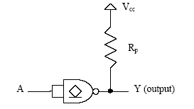
An open collector gate is much simpler; it consists of only one switch and no resistor, as in Figure 4.3.

ttl open collector output

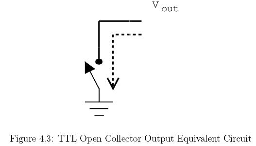
In essence, it only provides low outputs, and relies on an 
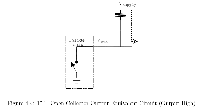
external pull up resistor to supply high outputs, as shown in Figure 4.4. The gate will not function properly without the external pull up resistor. Thus the gate is only ever used to sink current, and so can be optimized for that function.
ttl open collector output with pullup


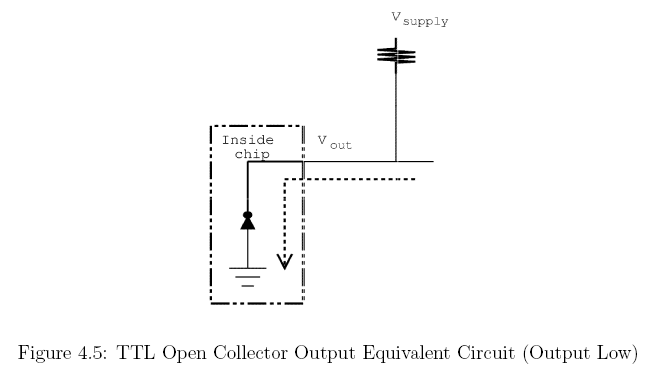
The big advantage to the open collector gate is that it can be used to provide much higher currents, since it only needs to sink them, not source them, as in Figure 4.5.
ttl open collector output low

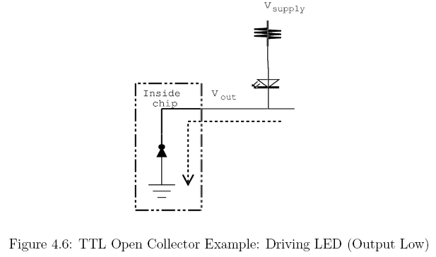
An example of this in use is to drive an output device like an LED which may require more current than normally provided by a TTL gate, as in Figure 4.6.
ttl open collector output with LED

Another possibility with open collector outputs is to drive devices which require a higher voltage than Vcc. Since the gate only needs to sink current, then the voltage connected to the output resistor can be anything, so long as it does not overload the sinking ability of the gate when the output is low. Thus, an open collector gate gives flexibility in output voltage and current for the cost of a bit of extra wiring.

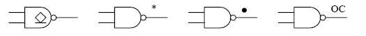
Open collector gates (and open drain gates) typically use one of the following symbols.

ttl open collector symbols

Equipment

Procedure

You will have to calculate pull-up resistor values for a number of the following circuits. See Pull-up resistor calculation for instructions on calculating the minimum and the maximum resistor values.

When looking up VOHmin, you'll need to look at the datasheet for the 74LS00, not the 74LS01. It's the value for the family that matters.
(In fact, the 74LS01 probably doesn't give a value for VOHmin. Why is that?)

Calculating Pullup Resistor Values

  1. Connect a 74LS01 open collector NAND with its inputs tied together (to act as an inverter) with no load and no pull-up resistor as shown below. Measure the output voltage for both HIGH and LOW inputs. Are the output voltages within the data sheet's specified ranges? (They should not be!) Record both your output voltage and the specified voltage.
    ttl open collector output without pullup

  2. For the following circuit using a 74LS01 open collector NAND gate, calculate the minimum and maximum values for a pull-up resistor assuming that there will be no load.
    ttl open collector output pullup

  3. Using an appropriate pull-up resistor, construct the above circuit. Record the value of resistor used. Measure the output voltage for both HIGH and LOW inputs. Are the output voltages within the data sheet's specified ranges? (They should be!)

    Demonstrate the operation to the lab staff.

Wire ANDing Open Collector Gates

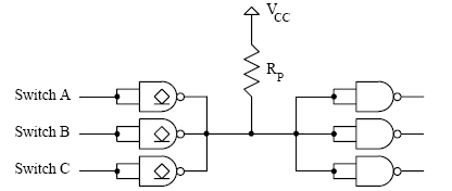
One of the possible uses for open collector gates is to allow wire ANDing of the outputs. This can reduce the number of components in certain circuits. With normal gates, you would need to use AND gates to combine the outputs. You will examine both situations.


caution

Caution! The following step uses a wired-AND configuration with a totem-pole output TTL gate.
If the power is applied to the circuit for more than 2 to 3 seconds, the gates will be destroyed.

NEVER do this in a real circuit!


  1. Connect the following circuit using a 74LS00 NAND. Please note that this circuit using a wired-AND configuration with a regular TTL gate. Power the circuit for only 2 or 3 seconds and measure the output voltage and current. You may have to measure them separately. Is the current within specified limits for a LOW output?
    Remember that if you're using an oscilloscope or a digital meter, the ground for the measuring device must be the same as the ground for the circuit.

    totem pole outputs

  2. For the following circuit using two 74LS01 open collector NAND gates, calculate the minimum and maximum values for a pull-up resistor, Rp, assuming that there will be no load. Please note that there are two input gates.

    ttl outputs

  3. Connect the above circuit using an appropriate pull-up resistor. Record the value of resistance used. Measure the output voltage and current. Are the current and voltage within specified limits for a LOW output? Why is the output LOW and not HIGH?

    Demonstrate the operation of your circuit to the lab staff.

Wire ANDing Example

  1. For the following circuit, calculate the minimum and maximum values for the pull-up resistor, Rp.
    ttl wired and outputs

  2. Construct the above circuit using an appropriate pull-up resistor. Record the value of resistance used. Note that the 74LS00 NAND gates are simply in the circuit to provide load. Determine the truth table for the circuit (excluding the load). Verify the truth table by measuring the voltage before the load. Are the outputs of the open collector gates ANDed together as predicted?

    Demonstrate the operation of your circuit to the lab staff.

Resources

To view pdf documents, you can download Adobe Acrobat Reader .
get Acrobat Reader
If you need to update a browser, you might try Firefox which is Get Firefox!
Since this page uses cascading style sheets for its layout, it will look best with a browser which supports the specifications as fully as possible.

If you are looking for an office package, with a word processor, spreadsheet, etc., you might try LibreOffice which is Get LibreOffice!

Go to the main page for the Department of Physics and Computer Science.

Valid XHTML 1.1

Valid CSS!

WCAG
2.0
(Level AA)

Wilfrid Laurier University