PC/CP200 Electronics Lab I
Logic Gate Characteristics - Voltages,
Propagation Delay, and Temperature
Objectives
- To measure the voltage characteristics for various digital
logic families.
- To measure the propagation delay for various digital logic
families.
- To obtain and interpret information from a data sheet.
Preparation
The operation of an ideal logic gate can be
summarized by
the following rules:
- Input and output voltages will be at either the high
or the low value specified for that family; (e.g. 5 and 0 volts,
respectively for LSTTL).
- Inputs will draw no current from whatever drives
them,
and outputs can supply as much current as necessary for whatever
follows.
- Any change of an input will immediately be effected
on
the output.
In practice, these rules do not hold. A real logic
gate
operates under the following restrictions:
- Input voltages will not always be at their ideal values, and
so a range of input values must be considered high and another
range of input values must be considered low. Similarly output
voltages will not always be at their ideal values, and so a range
of output voltages should be considered as high, while another
range of output voltages should be considered low.
- Inputs must draw a small but finite amount of current from
the driving devices and outputs have a limited current capacity
for maintaining the output voltage at the desired level.
- Changes made at the inputs will take a finite amount of time
to be effected on the outputs.
Note that in most labs comparing "real" to
"ideal" values involves seeing how close one number,
(the "real" value) is to another (the "ideal"
value). With digital logic chips, however, rather than having a
single "ideal" value for a parameter, the manufacturers
give parameter bounds. These specifications are not values that
should be matched, but rather they are values that should be
considered as limits during real operation. For instance, LSTTL
logic
has a nominal input "high" voltage of 5 volts, but in
practice any voltage above 2.0 volts will be considered
"high". Normally, voltage parameters will be different
for input and output. For the same LSTTL logic family, a
"high" output will be any output voltage above 2.7
volts.
Note that for some parameters the specifications will give an
upper bound, for some they will give a lower bound, and for others
they will provide a range. Which one is given will make sense if
you understand what each parameter means.
Supply Voltages
Digital logic chips have a power pin(s) and a ground pin(s).
These supply voltages have names which are based on the type of
transistors used in the construction of that particular logic
family.
- TTL gates are made with bipolar transistors, which have a
collector and an emitter; so the
supply
voltages
are shown as VCC (power) and Ground
(occasionally shown as VEE) on most
data sheets.
- CMOS gates are built with field-effect transistors, which
have a drain and a source; so
the
supply
voltages
are shown as VDD (power) and
VSS (ground) on most data sheets.
Voltage Characteristics
The voltage characteristics of a logic gate depend on the logic
family used to construct the device and are always specified on the
device data sheet. The voltage characteristics are always specified
in terms of four values:
- VIHmin -- the minimum input
voltage which will be accepted as a logic 1 state.
- VILmax -- the maximum input
voltage which will be accepted as a logic 0 state.
- VOHmin -- the minimum output
voltage representing a logic 1 state.
- VOLmax -- the maximum output
voltage representing a logic 0 state.
The following diagram shows these voltage characteristics for
five types of chips: two families (TTL and CMOS) with various
supply voltage characteristics (two high voltage and three low
voltage variations). All properly operating chips must work within
these ranges. For example, if both inputs to a 74LS00 TTL NAND gate
are greater than or equal to 2.0 volts, they will be considered
"high" and the output should be "low", i.e.
at a voltage less than or equal to 0.5 volts. Notice that the
output range, either high or low, is always smaller than
the
input range.
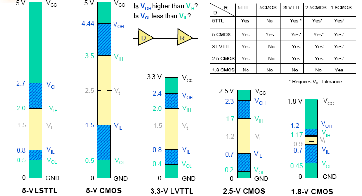
Texas Instruments, Logic Selection
Guide, 2003 (modified for LSTTL)
For high voltage CMOS logic (second from left in above diagram),
the supply voltage VDD can actually
range from 3.5V to 15V. The diagram only shows the voltage
characteristics at a supply voltage of 5V to allow comparison to
the 5V LSTTL characteristics. Read the data sheet for voltage
characteristics at supply voltage values greater than 5V.
Propagation Delay
Ideally changes to the inputs of a gate would be effected at the
output immediately, but in reality there is a slight delay. In
addition, the delay may be different depending on whether the
gate's output is going from low to high or from high to low.
Furthermore, the transitions themselves are not instantaneous, so
they are defined as being at the 50% point of the voltage
transitions. Thus there are two quantities of interest:
- tPLH -- the time interval between
the change of an input and the resulting change in output, when
the output must change from low to high.
- tPHL -- the time interval between
the change of an input and the resulting change in output, when
the output must change from high to low.
Note that in both cases above, the direction of the input
transition is immaterial.
Equipment
Procedure
 Great care should be taken to avoid static
discharge into CMOS (static sensitive) based chips.
Great care should be taken to avoid static
discharge into CMOS (static sensitive) based chips.
Before starting the lab, review the CMOS handling
procedures.
- Always use a ground strap. If your grounding mat doesn't
have two grounding straps, one for each of the partners, see the
lab instructor.
- CMOS devices should be stored pin down in conductive foam
when they are not in a circuit.
- Never leave unused inputs floating; connect to ground or +5V
to prevent excessive current consumption and erratic
behaviour.
- Never connect an input signal to a CMOS device when the power
is off.
Voltage Characteristics
Do the following analysis first for the 74LS00 and then repeat for the 4011. Before starting, determine
which of these chips is CMOS.
- From the data sheet, fill in the specified limits for
the quantities in Table 1:
| Table 1: Comparing voltage limits with
specifications
|
| parameter |
VIHmin |
VILmax |
VOHmin |
VOLmax |
| LS TTL
|
| specification |
|
|
|
|
| observed |
|
|
|
|
| within spec.? (y/n) |
|
|
|
|
| CMOS
|
| specification |
|
|
|
|
| observed |
|
|
|
|
| within spec.? (y/n) |
|
|
|
|
- Connect
the function generator (input) to channel 1 and the device
(output) to channel 2.
Make sure both the function generator and the oscilloscope have
the same ground (oscilloscope ground not shown in diagram).
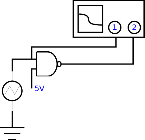
- For the function generator, select a 0 to 5V sine wave with a
frequency of 1 kHz. For the oscilloscope, select the X-Y mode of
operation. A trace similar to the one shown below should be
obtained. This is called the transfer characteristic of
the gate. Note that the input voltage, Vin, is on the X
axis and
the output voltage, Vout, on the Y axis.
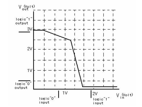
- Measure the values of the following parameters and
fill them in the "observed" cells in Table 1 above.
Specifically, you want to answer the following
questions:
- What output voltage is produced by an input voltage of
the specified value of VILmax?
This would be the measured value of
VOHmin. Is it within the manufacturer's
specifications?
- What output voltage is produced by an input voltage of
the specified value of VIHmin?
This would be the measured value of
VOLmax. Is it within the manufacturer's
specifications?
Compare the specified and observed values to
see whether the devices fit the manufacturer's
specifications and complete the "within spec" cells for each
quantity.
Demonstrate and explain your measurement and
conclusions to lab
staff.
Propagation Delay
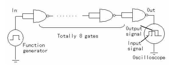
Do the following analysis just for the 4011.
- Using two 4011 chips, construct the circuit shown below. Use
a chain of 8 gates (n=8) to determine the propagation
delay tP. In order to obtain a good
measurement of the delay time, a frequency of operation should be
chosen sufficiently high so that the total delay in the chain
(ntP) is comparable to the
period of the input clock. Obtain the delay times
tPHL and tPLH from the
data sheets. Use the oscilloscope to measure Vin and
Vout.
Use a
square wave as input.
Note: You don't want to be in XY mode for this
part.
Why can we not measure both tPHL and
tPLH from the circuit shown? [Hint:
how many gates do we have and what is the relationship between
the input and the output?]
- The propagation delay of a CMOS gate is a function of the
load capacitance and the supply voltage VDD.
Determine the propagation delay tP as a function
of VDD.
Use a variable power supply and measure with VDD at
5V, 10V, and 15V.
When using different values for the supply voltage, be sure to
adjust the amplitude of the square wave input voltage
appropriately. Remember that the voltage required to
obtain a "high" changes as the supply voltage
changes.
The voltage diagram in this lab (in preparation
section) only shows the voltage characteristics at a supply
voltage of 5V to allow comparison to the 5V LSTTL characteristics.
Read the static electrical characteristics in the data sheet for
voltage characteristics at other supply voltage values.
Note, these are input voltages that can be read as exact values
from the table; you do not have to figure it out from the
graphs.
Demonstrate and explain your measurement to lab
staff.
- Plot a graph of propagation delay as a function of supply
voltage, labeling everything appropriately.
- How do your results compare to the device data
sheet?
Temperature and Supply Voltage
Characteristics
For both the 74LS00 and the 4011:
- What range of power supply voltages is allowed for normal
operation of the chip?
- What range of power supply voltages is guaranteed not to
destroy the chip?
- Over what range of temperatures may the chip be expected to
operate normally?
- Over what range of temperatures may the device be stored
safely?


