Pages created and updated by
Terry Sturtevant
Date Posted:
May 12, 2017
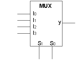
For this lab consider a MUX with one output and four inputs, where one of the four inputs must be selected for output through 2 selection lines.

Suppose these are the signals going in on each of the inputs, from
I3 to I0:
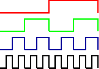
If the select inputs are set to 0, the output will be:
![]()
If the select inputs are set to 1, the output will be:
![]()
If the select inputs are set to 2, the output will be:
![]()
If the select inputs are set to 3, the output will be:
![]()
So if the select inputs cycle through all four possibilities,
the output will be:
![]()
Certain chips, like the multiplexer here, have "extra" inputs which allow more control over the outputs. With this multiplexer, there is a pin called strobe. This pin has to be connected correctly for the device to work as expected. Look at the device truth table to figure out whether this pin needs to be tied high or low.
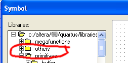
You will use
Altera Quartus II
to draw your
circuit diagram, and use the 74153M multiplexer from the
others | maxplus2
library.
Quartus II may use different pin names than the
datasheet (from ON Semiconductor)
or the lab writeup. You should be able to figure out which
pin maps to which based on the number and function of the various
pins.
Simulate your circuit to confirm that the multiplexer works as expected.
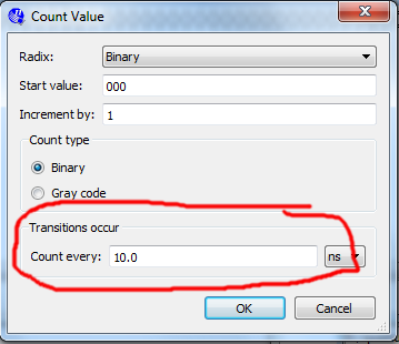
Hint: Look at the inputs to the multiplexer and see if there are
logical ways to group the inputs. You can make more than one input group
in Quartus, and not all of the inputs need to be in a group.
Note that you can change how fast a group counts with the value in the
"Count every" field.
Copy your directory from the E drive to the I drive.
Demonstrate the circuit to the lab demonstrator.
Delete everything from the E drive so your files don't get used by someone else later.


![]()
Wilfrid Laurier University
© 2019 Wilfrid Laurier University